Verify and complete the design of LCD large screen splicing system based on Xilinx Virtex-4 FPGA development platform
With the continuous improvement of the quality of various graphics and image content and the need for real-time display of the system, more and more industries such as finance, communication, transportation, energy, security, military, etc. need to establish a large screen that can integrate multiple signal inputs in real time. display system. The rapid development of digital technology has also enabled people to meet the needs of large-size, multi-picture, true color, high-quality, high-resolution computer graphics, graphics, data and various video image display effects. Among them, the demand for video information is the strongest. People not only hope that the video display size is larger and larger, but also the video display quality is required to achieve multi-picture, true color, high image quality and high resolution.
In the large-screen splicing system, the quality of the splicing controller directly determines the effect of the whole large-screen display system. At present, there are three implementation methods of the splicing controller: the working principle of the first-generation PCI plug-in type is Through the industrial computer, using a multi-channel PCI computer motherboard, a part of the PCI slot is inserted into the video capture card, and another part of the PCI slot is inserted into the video output card. The CPU is used to construct an operation and processing center between the input and the output, and then the group is built. An industrial control controller. The principle of his graphics processing is to divide the mother signal into M*N sub-video signals after the CPU operation, and then each sub-signal is amplified and transmitted to each corresponding unit on the wall of the splicing screen, and the display unit transmits the processor. The incoming signal is implemented on each display unit of the large screen, and the resolution and processing speed are determined by the computer CPU and the corresponding PCI card, so performance is limited. The second generation of embedded splicer is also called "internal splicer". It is based on the increased computational segmentation technology on the LCD signal driver board. Its working principle first transfers a complete mother image to the signal operation processor. The device starts to lock the position in the mother screen by means of the ID address encoder, and starts to operate into a plurality of sub-pictures in the order of the binary BCD code, and the processor directly supplies the respective calculated data to the liquid crystal driving board, and the driving board will Color, brightness, contrast and other parameters are adjusted and transmitted to the LCDIC imager to form an image in LVDS mode. The internal spelling splicer is only the processing of the internal display pixels of the unit. The result is a composite display image, which cannot solve the high-resolution stitching and arbitrary position of the signal. Multi-window signal processing of any size. The third-generation splicing system uses a pure hardware processor FPGA array processing architecture, full hardware design, no CPU and operating system. The controller integrates high-end image processing technology such as ultra-wideband video signal acquisition, real-time high-resolution digital image processing, and two-dimensional high-order digital filtering, and has powerful processing capabilities. The controller adopts multi-bus parallel processing mechanism, which can guarantee the full real-time processing of all input video fundamentally. The image has no delay and no lost phenomenon. Because it is structurally beyond the design concept of the first two generations of machines, pure The hardware processor technology, so the startup time is fast and the work is very stable.
In the digital system products, the ultra-large-scale, ultra-high-speed Field Programmable Gate Array (FPGA) is used to achieve hardware monolithic integration based on its high integration, high speed, and programmable advantages. trend. FPGA's rich internal resources and high speed provide solutions for real-time video processing.
Therefore, this project designs an FPGA-based digital video processing algorithm to decode DVI video signals, real-time segmentation of digital video, interpolation and amplification of video images, and simultaneously send the processing results to the LCD display via DVI encoding to complete the large screen. The design of the splicing system.
I. 1, system overview
1.1 system structure
The entire LCD screen display splicing system includes a DVI decoding module, a video segmentation module, an SRAM, a video extended linear interpolation amplification module, a video output control module, and a DVI coding module. The FPGA internal logic implements the input digital video into four parallel sub-video pixel streams, which are subjected to real-time interpolation and amplification processing through separate video processing channels. The video encoding circuit outputs a video display on a splicing screen composed of four LCD screens. The system structure design scheme of the application system hardware platform is shown in Figure 1.
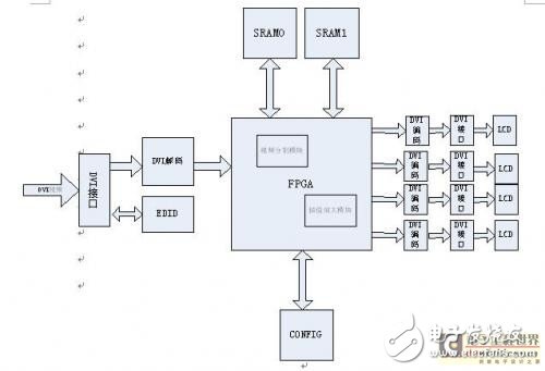
Figure 1 LCD screen splicing system structure
1.2 system principle
The LCD screen splicing display system works. The system receives a DVI digital video signal. Before processing, it needs to decode the video signal in the form of minimum transformed differential signal (TMDS) to obtain the pixel stream information that the FPGA can process. After video segmentation, the divided sub-video is combined with the generated reference video stream, so that the line field synchronization control signals of the respective sub-videos are consistent, and each sub-video is subjected to extended linear interpolation and amplification processing to obtain a digital video signal with a minimum transformed differential signal. Output to the spliced ​​LCD display via the DVI interface for display.
2, the function of the algorithm
The main functions of the algorithm are as follows: The FPGA digital video processing circuit is the logic for digital processing of video data, realizing real-time video pre-processing, image segmentation, video image interpolation and amplification, etc., and controlling four parallel segments through the video output module. The video is displayed synchronously on up to 4 LCD splicing screens. Has the following main features:
(1) receiving video image data sent from the DVI decoding circuit through the internal logic input module (VGA Input), including pixel data (R, G, B components) and video synchronization control signals (HSYNC, VSYNC), etc., converted into Preprocessed video pixel stream format.
(2) The video segmentation module implements the segmentation and trimming of the original single-frame video image, and obtains four complete video sub-pixel pixel streams (including video pixel data and video synchronization control data), and controls the mutual timing relationship of the four sub-video displays; The scanning points of the pixels of the splicing screen are the same, and are all in the form of progressive scanning, and the sub-video pixel points display synchronization, that is, line synchronization and field synchronization.
(3) The video interpolation module implements 2&TImes; 2 times interpolation and amplification processing for the sub-video obtained by video segmentation, the module adopts parallel processing mode, and the four-way sub-video respectively passes through independent video processing channels; the interpolation amplification algorithm is based on FPGA Perform extended linear interpola (TION) data calculation of the pixel to be interpolated, cooperate with the reference video stream generated by the video generation module (VGASyncGen), and implement time-division read-write switching of the interpolated pixel data through the shared line buffer memory. . The resulting video pixel stream contains the full video pixel stream format and meets the higher resolution video display requirements.
The pixel stream, the time that the serial pixel stream reads one frame of pixels is equal to the time that the input video pixel stream is written to one frame of pixels. The pixel stream fusion operation selects a video pixel with an offset under different clocks by setting a control parameter (control) on the input four-channel video.
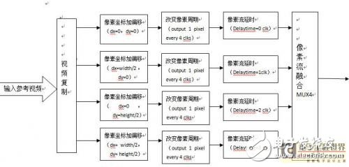
Figure 3 video logic control logic diagram
3.2 FPGA implementation of video interpolation amplification algorithm
The video interpolation amplification module includes a coordinate calculation unit, a weighting coefficient generator, a vertical interpolation unit, a virtual pixel buffer and a horizontal interpolation unit, as shown in FIG. 4:
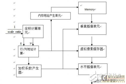
Figure 3 Block diagram of the interpolation amplification module 3.2.1 coordinate calculation unit
Extended linear interpolation requires 16 pixel points around the source image interpolation point, and then the coordinates of the interpolation points obtained from the parallel computation unit. The coordinates of the interpolated points can determine the coordinates of the adjacent 16 rows and column points, and then 16 pixels of pixels can be obtained from the memory and linear interpolation is performed.
The principle of linear interpolation can be decomposed into vertical and horizontal interpolation. For example, in Figure 4, the pixel in the horizontal direction is the address of the first virtual pixel, which enables the virtual pixel to be correctly read from the virtual pixel buffer. Interpolation in the horizontal direction. Such an operation does not require the circuits to be executed at the same time, so only one row or column of address calculation circuits is required.

Figure 3 Interpolation in the horizontal and vertical directions
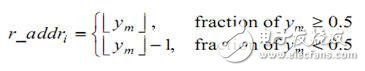
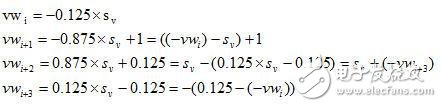
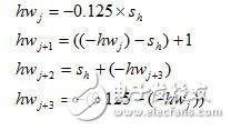
For column or row address calculators, the input signal determines the coordinates of the horizontal and vertical directions. The coordinate data contains a 10-bit real number and a 10-digit fractional part. The 9th bit of the coordinate data is the most significant bit of the fractional part, which determines whether the fractional part is greater than 0.5. At the same time, the multiplexer controlled by the 9th bit is used to output the correct memory address. If the input is a column signal, then the row address ![]() ,
, ![]() ,
, ![]() ,
, ![]() And vertical spacing
And vertical spacing ![]() Can be obtained by formulas (1) to (3), similarly, column address
Can be obtained by formulas (1) to (3), similarly, column address ![]() ,
, ![]() ,
, ![]() ,
, ![]() And horizontal spacing
And horizontal spacing ![]() Can be obtained by equations (1), (2) and (4).
Can be obtained by equations (1), (2) and (4).
(1)
![]() (2)
(2)
![]() (3)
(3)
![]() (4)
(4)
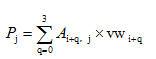
3.2.2 Weighting coefficient generation unit
In the block diagram of the design, the calculation of the horizontal weighting factor and the vertical weighting factor is not simultaneous production although they are all determined by equations (5) and (6). Therefore, the weighting coefficient generator generates horizontal and vertical weighting coefficients. When the control signal is a horizontal signal, the final output is ![]() ,
, ![]() ,
, ![]() ,
, ![]()
, on the contrary, the output ![]() ,
, ![]() ,
, ![]() ,
, ![]()
. The largest computational amount in extended linear interpolation is the calculation of weighting coefficients, while the most complex operation consists of the simplest two adders and two subtractors.
(5)
(6)
3.2.3 Horizontal and vertical interpolation units
According to equations (7) and (8), horizontal and vertical interpolation have the same operation, but they are performed in parallel to increase the overall speed. The logical structure of horizontal and vertical interpolation is shown in Fig. 5. The multiplier and the adder can effectively complete the convolution of the input data and the corresponding four weighting coefficients to generate the interpolation circuit.
 (7)
(7)
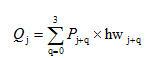 (8)
(8)
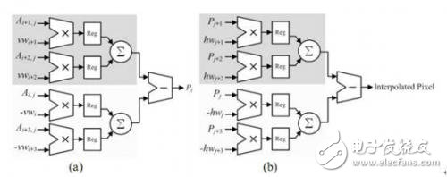
Horizontal interpolation unit vertical interpolation unit
Figure 5: Horizontal and vertical interpolation unit logic block diagram
3.2.4 virtual pixel buffer
Virtual pixel points are generated by vertical interpolation and stored in the virtual pixel buffer, which is called during horizontal interpolation. In general, the scaling determines the rate at which the buffer inputs and outputs data. When zoomed in, each virtual pixel is reused for horizontal interpolation so that the vertical inserter data rate is lower than the horizontal, as opposed to When zooming out, the virtual pixels are generated by the vertical interpolation process more than the horizontal interpolation process requires. In order to adjust different data rates, the virtual pixel buffer is designed as shown in FIG. 6, which includes one counter, eight registers and a buffer output control circuit. In the process of interpolation and amplification, the buffer sometimes delays vertical interpolation, and when the number of virtual pixels is larger than the determined number of horizontal interpolations, the generation of virtual pixels is stopped. The counter records the column address of the newly generated virtual pixel and stores it in reg7. Comparator and selector compare counter and ![]() The value determines the output of the buffer.
The value determines the output of the buffer.
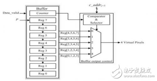
Figure 6 virtual pixel buffer
4, verification
The algorithm is verified based on the Xilinx Virtex-4 FPGA development platform. The video segmentation module and the extended linear interpolation module are respectively simulated to verify the correctness of the algorithm. After repeated optimization and testing, the algorithm is finally downloaded to the development board to verify the output. Whether the video display effect can meet the application requirements of video amplification, complete the design of the LCD large screen splicing system.
CCTV Power Supply,CCTV Power Supply Box,CCTV DC Distributed Power Box
Chinasky Electronics Co., Ltd. , https://www.cctv-products.com