Compact regular hexagonal DGS low pass filter design detailed tutorial
Defected Ground Structure (DGS) is one of the hotspots in the microwave field. It is developed from the photonic band gap structure (PBG). DGS etches the defect pattern on the ground plane to change the distribution of the shield current on the ground plane, thereby indirectly changing the equivalent inductance and equivalent capacitance of the transmission line to obtain slow wave characteristics and forbidden band characteristics. The slow wave characteristic makes the structure of the microwave transmission line more compact, and the forbidden band characteristic can suppress unwanted signals such as harmonic clutter. This technology has now been applied to filter design, making the filter's ability to suppress harmonics more prominent.
In this paper, a hexagonal ground defect structure is proposed as the basic unit of DGS. The designed DGS unit structure, whose unit equivalent circuit can be represented by the RLC parallel resonant unit, can easily control the equivalent inductance and capacitance by changing the area of ​​the regular hexagon of the ground defect unit and the width of the slot. Thereby adjusting its frequency response characteristics. In this paper, the equivalent circuit of the corresponding low-pass filter is proposed by studying the variation of the hexagonal size parameters. A filter based on five regular hexagonal DGS is designed. The simulation results of the equivalent circuit in ADS and The simulation results in HFSS are very consistent.
2 regular hexagon DGS low pass filter2.1 DGS and its equivalent circuit
The structure of the regular hexagonal DGS unit is shown in Fig. 1(a). Two symmetrical regular hexagons are etched on the ground plate below the microstrip line and connected by a slot. A substrate having a dielectric constant of 3.2 and a thickness of 0.787 mm is used herein. The 50Ω microstrip line length d is 1.88 mm, and the equivalent inductance L formed by the etched areas on both sides of the microstrip line and the equivalent capacitance C formed by the intermediate slots constitute the frequency response of the LC parallel resonant circuit to generate poles at specific frequency points. . Its lossy equivalent circuit is a parallel resonant RLC circuit. As shown in Figure 1(b), the RLC circuit consists of an equivalent shunt capacitor C, a shunt inductor L and a resistor R [7, 8]. These parameters can be extracted by EM simulation of the structure and the following formula
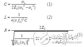
Where ω0 is the resonant angular frequency; ωc is the 3 dB cutoff angle frequency; Z0 is the characteristic impedance of the transmission line, where Z0 is 50 Ω.
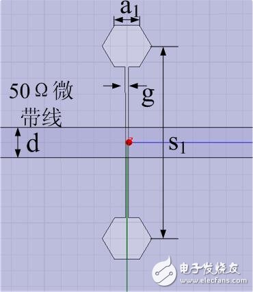
(a) Regular hexagonal DGS unit

(b) equivalent circuit
figure 1
The hexagonal DGS unit of Fig. 1(a) is modeled in HFSS for EM simulation, and the resonance frequency is observed as the side length of the hexagon changes. Among them, the length of the etched slot is s=12 mm, the width g=0.2 mm remains unchanged, and the side length of the hexagon varies from 1.0 mm to 2.5 mm. From the simulation results, it can be seen that the middle of the DGS pattern The width of the slot is constant, the equivalent capacitance is basically unchanged, and the equivalent inductance increases with the area of ​​the regular hexagon [5]. As the available 3 dB cutoff frequency is reduced, the resonant frequency of the LC resonant circuit is correspondingly reduced from 6.32 GHz to 4.43 GHz, as shown in Figure 2.
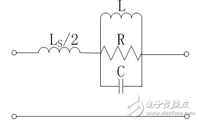
Figure 2 Effect of the length of the regular hexagon on the resonant frequency
2.2 Low-pass filter design
As can be seen from the above analysis, a regular hexagonal DGS structure can be used to design a low pass filter or to suppress parasitic sidebands. However, this structure also has some drawbacks, such as insufficient suppression in the high frequency range and a case where the cutoff characteristics are slow. Therefore, an H-shaped parallel branch is added to a single DGS unit to increase the coupling capacitance between the microstrip line and the regular hexagon DGS unit. This not only minimizes the size of the LPF, but also improves the stopband characteristics of the LPF. Figure 3 (a) is a DGS unit with H-shaped parallel branches, and (b) is its equivalent circuit.
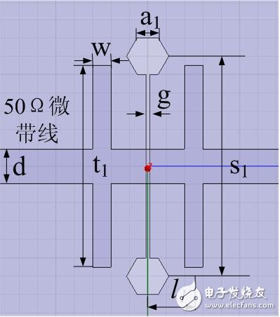
(a) DGS unit of H-shaped branch
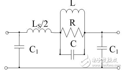
(b) equivalent circuit
image 3
Where l1 = 2.5 mm, w = 1 mm, a1 = 1.2 mm, d = 1.88 mm. In the case of other dimensions, the length t1 of the parallel branches gradually increases from 4 mm to 10 mm. It can be seen from the simulation results that as the l increases, the capacitance of the equivalent circuit also increases, thus the out-of-band The suppression is also increasing. The 3 dB cutoff frequency at 2.41 GHz does not translate, but the attenuation becomes deeper. When the length t1 of the parallel branch is 10 mm, the out-of-band rejection with respect to 4 mm is increased by almost 10 dB, as shown in Fig. 4.
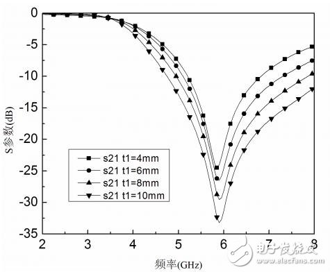
Figure 4 Effect of H-type slot length on resonant frequency
In order to obtain good frequency response characteristics and increase its out-of-band rejection, the number of regular hexagonal DGS units must be increased. The low-pass filter designed here uses five regular hexagon DGS units. Its symmetrical structure is shown in Figure 5(a), and the corresponding equivalent circuit is shown in Figure 5(b).
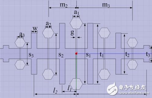
(a) LPF with five DGS units
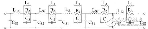
(b) equivalent circuit
Figure 5
With the exception of t3, other parameters are obtained by analyzing a single unit. Their dimensions are: w = 1 mm, g = 0.2 mm, a1 = 1.15 mm, a2 = 1.05 mm, a3 = 0.95 mm, s1 = 11 mm, s2 = 7.5 mm, s3 = 4 mm, l1 = 2.5 mm , l2 = 7.5 mm, l3 = 12.5 mm, m2 = 5.1 mm, m3 = 10.1 mm, t1 = 11 mm, t2 = 7.5 mm.
Figure 6 is a simulation result of a low pass filter using five DGS units as a function of the length of the parallel branch t3. As the length of the parallel branch increases, the equivalent capacitance CS3 shown in Fig. 5(b) also increases. This increases the out-of-band suppression and the attenuation of the pass-to-band resistance becomes steeper. At the same time, we also noticed that its in-band characteristics such as insertion loss and return loss have increased. Therefore, in the design process, both the passband and the stopband must be considered.
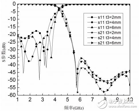
Fig. 6 Comparison of simulation results of LPF frequency response with t3 from 2mm to 6mm
The optimized low-pass filter characteristics can be obtained by simulation of EM simulation and equivalent circuit. When t3=3 mm, the simulation results are shown in Fig. 7.
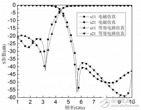
Fig. 7 Comparison of electromagnetic simulation and equivalent circuit simulation results of LPF
The corresponding equivalent network parameters are: C1 = 0.627 pF, C2 = 0.109 pF, C3 = 0.067 pF, L1 = 1.25 nH, L2 = 1.608 nH, L3 = 0.515 nH, R1 = 8.87 kΩ, R2 = 2.39 kΩ, R3 = 1.15 kΩ, CS1 = 1.238 pF, CS2 = 0.927 pF, CS3 = 0.303 pF, LS1 = 1.01 nH, LS2 = 0.802 nH, LS3 = 1.128 nH.
In order to verify the correctness of this equivalent circuit, the equivalent circuit was simulated by ADS. It can be seen from the comparison of the simulation results that the two agree well. For the frequency characteristics of the low-pass filter, the corresponding 3 dB cutoff frequency is 4.42 GHz, its S11 is lower than -21 dB in the passband range, and in the wide band of the stopband, from 5.5 GHz to 10 GHz. An out-of-band suppression of less than -40 dB can be obtained. The DGS structure using the H-shaped parallel branches can achieve higher attenuation and harmonic suppression in the stop band than the conventional DGS structure, while achieving steep drop characteristics.
3 ConclusionIn this paper, a low-pass filter based on a regular hexagonal DGS unit is proposed, and its out-of-band suppression is increased by adding an H-shaped parallel branch to increase its equivalent capacitance. The equivalent circuit model of the DGS low-pass filter is proposed. The equivalent circuit component value of the low pass filter is obtained by analyzing the size parameter of the DGS unit. A low-pass filter based on five regular hexagonal DGS elements is designed. The results of modeling and simulating in HFSS are basically consistent with the results of simulating the equivalent circuit in ADS. The cutoff frequency response is very steep and can achieve S11 below -2 dB with a cutoff frequency of 4.42 GHz. And a stop band rejection of less than -40 dB over a wide frequency range of 5.5 GHz to 10 GHz.
Distribution Box,Industrial Distribution Box,Electricity Switch Box,Box For Distribution
Guangdong Shunde Langzhi Trading CO., Ltd , https://www.langzhielectrical.com