Pfc circuit with mos tube need to pay attention to what matters?
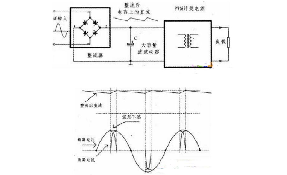
The figure above shows the schematic block diagram of the rectifier circuit that is not added to the PFC circuit. The figure below shows the working waveform. From the above analysis we can see. After the rectifier circuit that has not joined the PFC circuit works stably, only the diodes near the positive and negative peaks of the mains voltage are turned on to generate a pulse current. The reason that the power factor of the off-line power supply is reduced is that the conduction angle of the current is too small, which is much less than 180° in a half cycle. To increase the power factor, it is necessary to try to make the waveform of the current trace the voltage waveform throughout the entire cycle.
Since the reason why the conduction angle is too small is the large-capacity filter capacitor connected behind the rectifier, the basic idea of ​​the active PFC circuit is to add a primary adjustment between the rectifier and the large-capacity filter capacitor to isolate the two. The primary regulation converter outputs a substantially stable DC voltage, while its input current can be changed in the same sinusoidal pattern as the mains.
The circuit shown in the figure below is the basic structure and working principle of adding a PFC circuit. By comparison, we can clearly see the position and role of the PFC circuit in the power circuit structure. Although the specific forms of the PFC circuit are numerous and different, and the operating modes are also different (CCM continuous current type, DCM discontinuous type, CRM critical type), the basic structure is similar, and most of them adopt the boost boost topology. Because of this circuit form more advantages. This is also a typical step-up switching circuit. The basic idea is to divide the rectifier circuit and the large filter capacitor as mentioned earlier. By controlling the turn-on of the PFC switch, the input current can track the input voltage change. The working principle is not complicated. Thoroughly interpreting the basic circuit principle can be analogous to bypassing and laying the foundation for an independent analysis circuit. In this circuit. The PFC inductor L stores energy when the MOS switch 0 is turned on, when the switch is turned off. Inductor L induces a positive voltage and a negative voltage. The energy stored during the on-time charges the large filter capacitor through the boost diode D1 to output energy, but the input voltage is the unfiltered ripple voltage. It is worth noting that most of the flat panel TV's PFC inductor L is connected in parallel with a diode D2, which has a protective effect.
We all know that the large energy storage filter capacitor C and the PFC inductor L behind the PFC circuit are connected in series. Since the current on the inductor L cannot be mutated, the inrush current of the large filter capacitor C is limited.
Shunt protection shunt diode D2. Since there is no limiting effect of the inductance, the impact on the filter capacitor will be even greater, but it can protect the booster, especially the PFC switch. Dl is a fast recovery diode (because the switch is turned off when the inductor current is not zero, it needs to withstand more stress, requires a diode with very low or even zero reverse recovery current), and withstands inrush current Weaker. Reducing the reverse recovery current and increasing the surge voltage carrying capacity are mutual restraints, and the D2 uses an ordinary rectifier diode, and has strong ability to withstand inrush current, such as 1N5407 rated current 3A. Surge current up to 200A.
The surface of the protection diode D2 is reduced by the surge impact on the PFC inductor and the boost diode, but in fact there is an important role to protect the PFC switch tube.
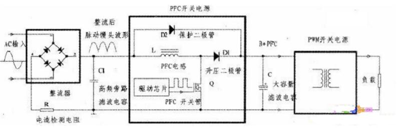
At the moment of starting up, the voltage of the filter capacitor has not been established yet, due to the need to charge large capacitors. The current through the PFC inductor is relatively large. If the power switch is turned on at the maximum value of the sine wave, the PFC inductor L may be magnetically saturated during charging of the capacitor. At this time, the PFC circuit will be in trouble if the magnetic saturation occurs. The current flowing through the PFC switch will lose its limit and burn the switch. To prevent the tragedy, one method is to control the timing of the PFC circuit operation, that is, when the charging of the large capacitor is completed, and then start the PFC circuit: Another simple method is to the PFC coil to the boost diode Connect a diode bypass in parallel. At the moment of starting, another branch is provided for charging the large capacitor to prevent the large current from flowing through the PFC coil to cause saturation. The overcurrent damages the switch tube and protects the switch tube. The protection diode D2 also shunts the current on the boost diode D1. The boost diode is protected. In addition, the addition of D2 speeds up the charging of large capacitors. The establishment of the voltage on it in time can also make the voltage feedback loop of the PFC circuit work in time, reducing the turn-on time of the PFC switch when starting. Make the PFC circuit work as soon as possible. Therefore, in summary, the role of the diode D2 in the above circuit is to provide a charging path for the capacitor at the moment of power-on or load short-circuit and the PFC output voltage is lower than the input voltage, so as to prevent the magnetic saturation of the PFC inductor from causing damage to the PFCMOS tube. The danger also reduces the burden on the PFC inductors and boost diodes and provides protection. After booting normally, because the right side of D2 is the output voltage of B+PFC, the voltage is higher than that of the left side, and D2 is reverse biased and cut off, which has no effect on the work of the circuit. D2 can be used with ordinary large currents that can withstand large surge currents. rectifier diode. In some power supplies, the capacitance behind the PFC is not large, and some do not have access to the protection diode D2. However, if a large-capacity filter capacitor is used behind the PFC, the diode cannot be reduced, which is of great significance to the safety of the circuit. .
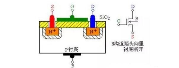
MOS tube structure and working principle 1, structure and symbols (in the case of N-channel enhancement type)Diffusion of two higher concentration N-type regions as a drain and a source on a lower concentration of P-type silicon, the semiconductor surface is covered with a silicon dioxide insulating layer and an electrode is pulled out as a gate.
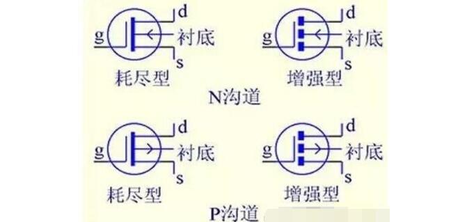
Other MOS tube symbols
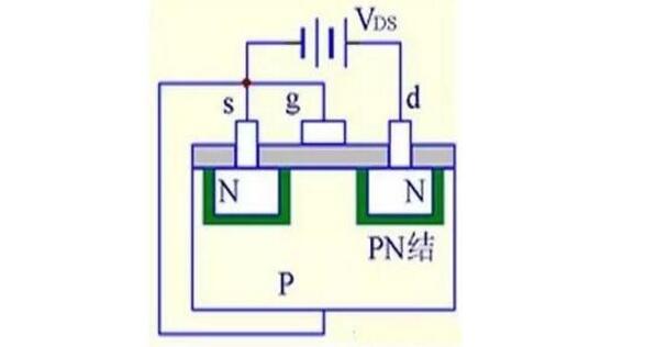
(1) When VGS = 0, there is no conductive channel because there is always a PN junction reverse bias regardless of VDS polarity.
VGS=0, ID=0
VGS must be greater than 0
The tube can work.
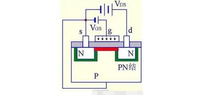
(2) When VGS ≥ 0, an electric field perpendicular to the semiconductor surface is generated in the Sio2 medium, repelling many sub-holes in the P region and attracting fewer electrons. When the VGS reaches a certain value, an inversion layer is formed on the surface of the P region to communicate with the N regions on both sides to form a conductive channel.
VGS> 0 → g attracts electrons → inversion layer → conductive channel
VGS↑→Inversion layer thickening→VDS↑→ID↑
(3) When VGS ≥ VT and VDS is small:
VDS↑→ID↑
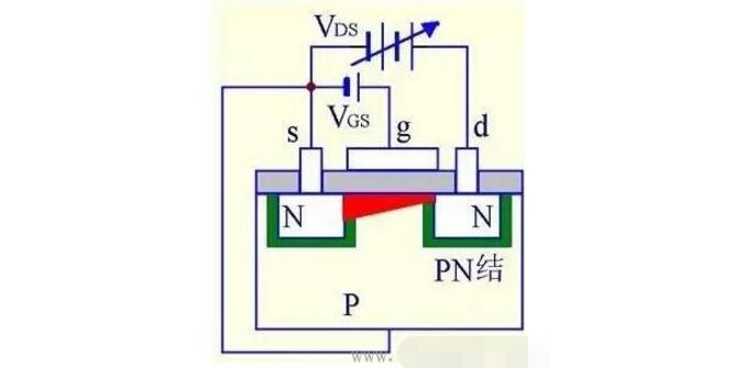
VT: turn on voltage in VDS
VGS° when starting to conduct with
VT=VGS-VDS
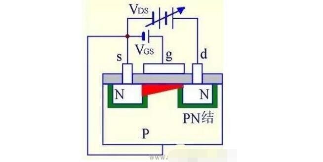
(4) After VGS is 0 and VDS increases to a certain value, the channel near the drain is pinched off, forming a pinch-off area.
VDS↑→ID unchanged
MOS PFC driver circuit design and precautionsThe PFC is one of the topologies in the power supply topology where the MOS requirement is relatively high. This is because: (1) The PFC has a relatively wide input voltage range. Most modern power supplies require a full range of AC voltages from 90-264V, which means that MOS must have sufficient voltage rating and can withstand large currents. (2) The control loop of PFC is slower in speed and is smoother. 100Hz/120Hz AC rectified ripple, PFC reaction time must reach tens of ms. If the control circuit and IC are not specially optimized, the starting process will often produce a large inrush current, the inrush current can reach 5-10 times of normal operation; (3) In the absence of undervoltage protection PFC, when the AC voltage drop Below a lot of 90V, the circuit still may continue to work, this will also produce the very high switch peak electric current, cause the interference and stress to exceed the normal range. Figure 6 shows a typical PFC circuit. Figure 7 shows the inrush current at the MOSFET drain when the PFC is started.
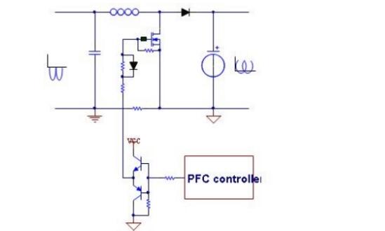
Figure 6: Typical PFC Circuit 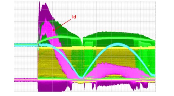
Figure 7: PFC Startup, MOSFET Drain Inrush Current
The MOSFET driver circuit has many mature solutions. In practical applications, many drive circuits use a relatively simple chip direct drive scheme for cost considerations. However, in applications with high power and performance requirements, the design of the driver circuit still has a great influence on the reliability of the MOSFET and the performance of the system.
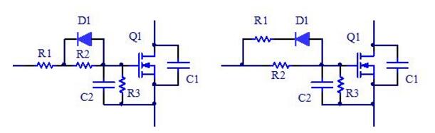
Figure 8: Two Basic Drive Circuit Structures for MOSFETs
Figure 8 is the most common MOSFET drive circuit, R1, R2 is Rg, the left picture R1 + R2 is the charging resistor when the driving voltage rises, R1 alone as a discharge resistor, right R2 alone as a charging resistor, parallel R1 and R2 As a discharge resistor. R3 drives the self-discharge resistor. C1 and C2 are additional Cds and Cgs capacitors, respectively.
(1) dv/dt control strategy and precautionsFactors that affect dv/dt are MOS characteristics, current peaks during switching, and Rg of the drive circuit. Since Cphas of AlphaMOS is particularly small, an appropriate increase in Cgs is also a way to effectively improve dv/dt.
Although the MOSFET itself can withstand high dv/dt and di/dt, empirical data shows that by changing Rg and Cgs, the control dv/dt does not exceed 20V/ns, and the corresponding di/dt does not exceed 200A/ns. The actual circuit can have a good working condition. When the efficiency allows, dv/dt is less than 10V/ns, and di/dt is less than 100A/ns, which is more conducive to reliability, as shown in Figure 9 and Figure 10.
In PFC applications, there are wide input voltage ranges, input voltage transitions, and slow response times, which can easily cause relatively large inrush currents. In this application, special attention needs to be paid to controlling the peak current. Under the same driving parameters, the higher the peak current, the larger the dv/dt and di/dt of the switch. The driving parameters should be adjusted according to the maximum peak current in the actual application. In the design, it is necessary to monitor the switching waveform at the maximum inrush current to determine whether it is necessary to adjust the driving parameters so that the MOSFET operates in a better state.
Dv/dt can also be easily reduced by adding additional capacitance to the drain. In the forward-active clamp, bridge-type soft-switch, and resonant circuits, the proper drain-source capacitance helps to optimize the switching state. In the PFC and flyback circuits, care must be taken to properly balance the efficiency. In the allowable range of efficiency, EMI can also be effectively reduced by increasing the drain-source capacitance.
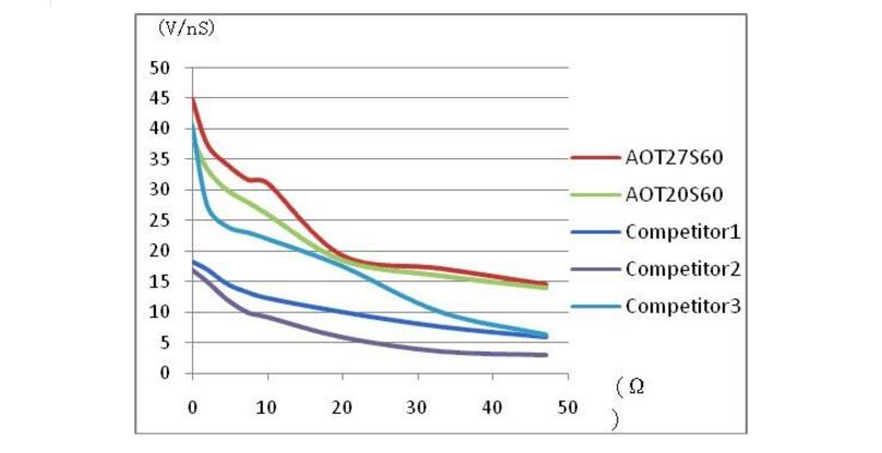
Figure 9: Relationship between MOSFET Turn-Off dv/dt and Discharge Resistance 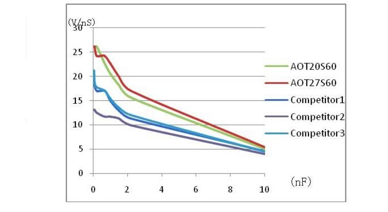
Figure 10: MOSFET Turn-Off dv/dt vs. Cgs
(2) Reduce the interference of driving through Cgd couplingDue to the high-speed switching characteristics of AlphaMOS, and the extremely low Ciss and Crss, AlphaMOS is more susceptible to layout failure and causes the driver to be disturbed. This interference is often due to the high frequency and high voltage traces being too close to the drive traces. The drain high dv/dt signal is passed through the coupled amplified Cgd into the drive signal. As shown in Figure 11 and Figure 12.
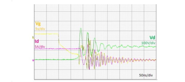
Figure 11: PFC MOSFET driver is disturbed 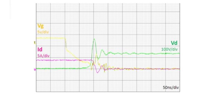
Figure 12: PFC MOSFET Driver Normal
(3) Magnetic beads added to the driverThe addition of magnetic beads at the drive end is a simple and reasonable method that can suppress spikes at the drive end that are subject to interference. It is recommended to place the beads as close to the MOS drive as possible. Plug-in packages such as the TO220 package can use ferrule beads. SMD packaged MOS can use SMD beads that are similar in size to chip resistors. Selecting magnetic beads needs to consult its data sheet to ensure that currents of at least 3A can be passed, and its peak suppression frequency should be 30-100 MHz. Under normal circumstances, the magnetic beads do not affect the driving waveform. The magnetic beads only work when a large current flows through the MOS and the interference suddenly increases.
(4) Reasonably place the drive componentsFor a driver circuit with a totem pole drive or a triode-assisted discharge, the circuit elements that assist and enhance the effect are as close as possible to the MOS. In particular, the ground wire should be directly connected to the source of the MOS. It must be avoided that the main power part of the ground loop on the drive is passed. Otherwise, the large current in the main power loop will be coupled to the drive loop. , causing the driver's accidental opening and erroneous shutdown. The drive signal of the control chip must be away from the high voltage and high frequency traces. Since the ground of the chip is often far away from the source of the MOS, only direct drive of the chip is used in low-power applications. For applications with high power or strong interference signals, it is recommended to use an auxiliary drive circuit with drive enhancement.
300w FM Transmitter equipment has a trigger signaltonoise ratio and low power consumption. Fm radio transmitter that can be used for factories, schools, supermarkets, farms, office space or create your own bad situation. And this fm radio transmitter that can be used for automatic detection of local wireless signals, easy to operate, and quiet. Fm radio transmitters are used to receive radio signals, so you have the stations in the car or on a boat. At the same time, this fm radio transmitter is a special handheld device that can be used to receive the signals in your car or home.
300W Fm Transmitter,300W Broadcast Transmitter,300W Audio Transmitter,300W Fm Broadcast Transmitter
Anshan Yuexing Technology Electronics Co., LTD , https://www.yxhtfmtv.com