Analyze some hardware related concepts in embedded development
Do embedded system development, often have to touch the hardware. Do embedded development to have a certain understanding of digital circuits and analog circuits. This will allow for in-depth research. Below we briefly introduce some of the hardware-related concepts in embedded development.
LevelIn the digital circuit, it is divided into high level and low level, which are represented by 1 and 0 respectively. The pin of a digital circuit always has a level, either high or low, or either 1 is going to 0 (in fact, there is another state, which will be mentioned later).
BusThere must be a processor chip in the embedded system. In addition, there are other chips as external devices (hereinafter referred to as peripherals), which cooperate with the processor to realize the functions of the product. Complex products are often made up of a large number of chips. Then it is inevitable that we need to connect all the peripherals to the processor. The simplest is to connect all the peripherals to the processor with independent (note independent) signal lines. The advantage is easy to understand. But the problem is: not feasible. Because the processor chip needs to draw too many lines, it is not practical from the point of view of chip production and product production. In addition, the processor (here we assume that the processor is single-core, not multi-core) processing transactions are microscopically serial, that is, if the peripheral is to be read or written at a certain time, it is only possible It is done for one of a large number of peripherals, that is, multiple peripherals cannot be simultaneously accessed by the processor at the microscopic level. It should be noted that the concept of micro is proposed here, which is to distinguish it from the macro. Macroscopically, there can be multiple tasks running simultaneously in a single processor, but these tasks are run one at a time microscopically (the serial will be used to describe the "one by one" here), multitasking The serial operation implementation is implemented by the operating system playing an important role. Back to our topic, it is not feasible to connect each peripheral with a separate signal line to the processor, and the processor will only access one peripheral in a single time, then we can use a shared signal line. Connect all the chips together? This is the origin of the bus concept. In layman's terms, if there are ten families around us, in order to allow each of the ten families to travel between each other, we do not need to build a separate (note separate) path for each of the two families (if so, Instead of repairing 45 roads, you can build a road, and then each home is connected to the main road.
For the bus, we often say that the bus is a processor, while other peripherals are attached to the bus. There is a problem. We can only access one peripheral connected to the bus every time. How do we distinguish these peripherals? Like our way, we need to use an address to distinguish each family. On the bus, we also use addresses to distinguish them. In this way, the bus is divided into two categories according to its function. One type is the address bus. The data on this bus will only be "streamed" from the processor to the peripheral and is unidirectional. The other type is the data bus, which is used to transfer data from the processor to the peripheral (write from the processor's perspective) or to transfer data from the peripheral to the processor (from a processor perspective) Is a read operation), obviously, the data bus is bidirectional. That is to say, in our embedded system, both the address bus and the data bus are connected to all the chips that need to communicate with the processor.
The bus is wide, just as our road is divided into "three lanes" or "four lanes". We say that 32-bit processors mean that the data bus width is 32 bits, that is, "32 cars can run at the same time. "Obviously, the wider the width, the faster the processor speed, because we can access data from peripheral chips faster, which is why our computer is moving to 64-bit." Similarly, the address bus is also wide, and for 32-bit processors its maximum width is 32 bits.
The concept of the bus has, then the next problem is, even if each peripheral has an address, then where is this address recorded? Is it on the peripheral chip? If this is the case, then there is a problem. The address of each type of peripheral must not overlap. When two identical chips are needed in a product, the addresses of the two chips cannot be distinguished. It seems that this operation There is a problem. Also, if so, each peripheral must be fully connected to (for example, 32) data buses, and listen to the data lines to see if the processor is "calling" itself, which is very complicated. In addition, the address may also be used up because of the variety of peripherals. In general, the address cannot be stored in the peripheral chip. How do you let the peripheral know that it is being replaced by the processor and needs to be read and written? The answer is the chip select (CS, chip select) signal, or the EN enable signal.
Chip selection (CS or EN)For the peripheral chip, the chip select signal is a (also a) notification signal, telling the chip "Hey, please open the door, I want to put something in, or take something to go", the only thing here is the data. It can't be a corn cob or something. There is a question, where does this signal come from? Obviously, it can only come from the processor. Is that also like a bus, each chip shares a line together? If so, it is possible that the processor "opens the door" and all the chips open the "door". If the processor is writing data, then all chips may be written with the same data. When fetching data, each peripheral chip "throws" the data outward, which will cause the data bus to conflict, because some chips "throw" 1 to the bus, and some "throw" 0. In this case, The processor must be "mad" because it doesn't know if it should get 1 or 0.
That being the case, obviously it is not possible to connect all the chip select signals together, only the chip select signals of each chip are independent. As mentioned above, the address bus, we use an address line to connect a peripheral chip? Still use other methods. If you use an address line to connect a peripheral chip, you may only be able to mount up to 32 chips, which is obviously not possible. In fact, in reality, a 32-bit number is used to represent the address of a peripheral chip. For example, 1 can represent chip A, and 6534 can represent another chip B, and so on. From this point of view, in theory we can represent 2 32 power (4294967296) devices, the reason is theoretical, because some devices take up a large number of addresses. That being the case, there is still a problem, if the 32-bit address bus is converted into a chip select signal of the chip? This requires the introduction of the concept of a decoder.
decoder)The decoder converts a data into a signal on a signal line. For example, a 3/8 decoder can convert a data with a bit width of 3 bits into 8 (2 to 3 powers) completely independent signal lines. When the binary 011 is written to the data side, it corresponds to the third root of the eight lines, and when the binary 111 is input, it corresponds to the last one of the eight lines. With the decoder, the processor's address line is simplified. As long as 32 address lines are added to the external decoder, a large number of peripheral chips can be accessed. We have already solved the problem of selecting external devices. Now we have to look back at the data bus.
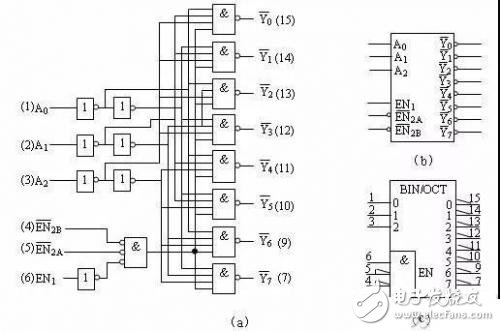
Figure 1 3/8 decoder
In an embedded system, the data bus of all chips can be understood to be directly connected. The reason why the word "understandable" is used is because the bus driver is added to increase the load capacity of the bus. To understand, let's take a look at the tap water in our lives. For example, in Beijing, all the water pipes may be connected together, but in the middle, in order to increase the water pressure, there are many small water stations to increase the water supply pressure. It is impossible for all the tap water in Beijing to come from a water plant. Now that all the data buses are connected together, there may be problems. When writing data to an external device, the processor first transfers the address of the target peripheral to the address bus, and the address decoder converts the chip select signal into a signal to the target peripheral, and the target peripheral receives the signal. , open the "door". Next, the processor will transfer the data to be transmitted to the peripheral device to the data bus. Since only the target peripheral chip opens the "gate", the data will only enter the target peripheral, and other peripherals will not receive anything. To. well! There should be no problem with the processor writing data out. Let's take a look at it. Read, because the data is sent from the peripheral to the processor, although we use the same method as the write to open the "gate" of the target peripheral, but at this time, other peripherals are also on the data bus, they may be in 1 may also be at 0, does it affect the processor to read the data of the target peripheral? The result is certainly not, but we have to introduce another concept: high resistance.
High resistance stateObviously, when the processor reads data from the target peripheral, we hope that the data bus of other unselected chips will not affect the data to be transmitted by the target peripheral. What should we do? In fact, when the chip is not selected, its data bus is in a high-impedance state. The so-called high-impedance state, we can understand that this pin is disconnected inside the peripheral chip, so obviously does not have any impact on the processor reading data from the target peripheral. We say that when a chip is not selected or not enabled, its data bus must be in a high-impedance state. In the front, I used the opening and closing of the "door" to make an analogy. What does the "door" mean? Refers to the data bus of the peripheral. The role of the chip select signal is to control whether the data bus of the peripheral is connected or disconnected from the data bus of the processor. For more explanations on high-impedance states, see the article "High-impedance and tri-state gates".
driveWhoever puts the data on the bus, we say who is the driver of that moment. That is, when the processor writes data to the peripheral, it is driving the data bus, and when the processor reads data from the target peripheral, the target peripheral is driving the data bus. For the address bus, the address bus is always driven by the processor because it is only possible to write from the processor to the target peripheral. When a chip is not selected, we say that it does not drive the data bus.
Tri-state gateEarlier we said that the data bus of the peripheral chip is in a high-impedance state when it is not selected. When it is selected, its level may be high (1) or low (0). As a result, we say that the peripheral data bus has its chip pins belonging to the three-state gate, that is, there are three states of high level, low level and high resistance state. For more explanations on the three-state gate, see the article "High-impedance and tri-state gates".
Level validityEarlier we learned what a chip select signal is, and also talk about the three-state gate. It should be pointed out that the chip select signal is usually not a tri-state gate. It only has two states, high level or low level. As we said before, the chip select signal is used to "open the door", and the chip select signal has high and low levels. In the end, is the high level indicating "opening the door"? Still low? For this problem, we say that if a level indicates "opening" for a chip select signal then it is the active level of this signal. For example, for a chip select signal, if the low level means "open the door", then we say that the chip select signal is active low. Although we use the chip select signal to explain the validity of the level here, many signals have validity problems. For example, the read signal and the write signal that we will talk about later have validity problems.
TimingEarlier we said that when the processor wants to write data to the peripheral chip, the address of the peripheral to be accessed needs to be placed on the address bus, and then the decoder converts the data on the address bus into a chip select. The signal, chip select signal enables the target peripheral chip, and then the processor writes the data onto the data bus to complete a write operation. Obviously, the data on the address line must remain for a period of time before the processor writes the data to the data bus. Otherwise, the decoder cannot validate the chip select signal for a long time. When the data write operation is completed, the processor does not need to ensure that the address on the address bus is valid. We can see that this series of operations has a strict chronological order, which is called timing. The timing describes the "procedure" of the interaction signal between the processor and the external device. Only by following this "procedure" can the normal communication between the processor and the external device be guaranteed. This is like a traffic light on our road. If our pedestrians and vehicles do not follow their instructions, an accident will occur. Typically, timing diagrams are used to describe the signal "procedures" for communication between chips.
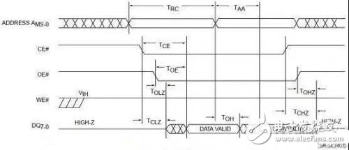
Figure 2 read timing diagram
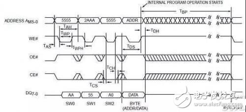
Figure 3 read timing diagram
From the figure we can see that ADDRESS is the address bus, DQ is the data bus, CE is the chip select signal, and it is active low, its width must be guaranteed to be valid during the read operation. Learning to look at the timing diagram is very helpful for doing embedded system development, because we inevitably have to deal with the chip. In the timing diagram, a lot of time requirement information is usually identified. When writing the startup code, it is necessary to initialize the chip select address register and read and write timing of each address space. The timing configuration is based on the time requirement of the peripheral chip, which is a very important part of the chip manual. When there are multiple peripheral chips in an address space, we need to consider the time requirements of the slowest peripheral chip. Otherwise, some chips will not work properly.
Read signalWhen the processor needs to read signals from the peripheral chip, in addition to the need to generate a chip select signal, it is also necessary to tell the peripheral chip that this is a read operation, not a write operation, which is achieved by reading the signal.
Write signalI read the read signal earlier. I think it is not difficult to understand the write signal. This signal is used to tell the peripheral chip. This is an operation to write data to the peripheral chip.
Special equipment for university physics laboratory
Teaching Equipment,Optical Bench Kit,Optical Instruments In Physics,Electrooptical Modulator Experimental Instrument
Yuheng Optics Co., Ltd.(Changchun) , https://www.yhencoder.com