Board-level packaging industry technology and market trend report
Memes Consulting: OSAT has been driving the semiconductor industry to develop innovative solutions, one that takes advantage of economies of scale and efficiency by switching from wafer and strip levels to larger panel levels. And board-level manufacturing can showcase the expertise and infrastructure of the photovoltaic industry with wafer-level packaging (WLP) and PCB flat panels.
Board-level package manufacturers are already preparing for mass production.
Why the industry favors board-level packaging
The need for lower cost and higher performance, coupled with OSAT (outsourced semiconductor packaging and testing) / assembly plant end customers continue to demand lower prices, has been promoting the semiconductor industry to develop innovative solutions. One option is to take advantage of economies of scale and efficiency by switching from wafer and strip levels to larger panel levels. The conversion from wafer level to board level (for example from 12-inch wafers to 18 x 24 inch panels) can be reduced by up to 50% (if the technology is complete) and the yield is over 90%. Moreover, board-level manufacturing can leverage the expertise and infrastructure of wafer level packaging (WLP) and PCB/flat display/photovoltaics.
According to Mamms Consulting, many factors are driving the development of board-level packaging (PLP), driving many vendors in all parts of the supply chain to invest in board-level infrastructure. On the one hand, leading fabless manufacturers want OSAT vendors to reduce the cost of high-density fan-out wafer-level packaging (FOWLP), and the use of large-sized panels seems to be the key to significantly reducing package price. In fact, all major OSAT vendors have a fan-out board-level package (FOPLP) on their roadmap. On the other hand, it is those who invest strategically, develop PLP capacity and actively promote their applications. These manufacturers are mainly driven by the success and promotion of FOWLP business, and also include:
- Those who missed the early boom of FOWLP (eWLP) (eg PTI Licheng Technology, ASE Sun Moonlight);
- Loss in the substrate business, and hope to develop a new business that can take advantage of its substrate manufacturing experience (such as SEMCO Samsung Motor, Unimicron Xinxing Electronics);
- already have panel-level process experience (such as LCD packaging) and believe they can apply these experiences to PLP (eg NEPES Naples);
- I hope to develop high-density, low-cost packages to support its front-end chip business (such as Samsung Electronics, Intel Intel).
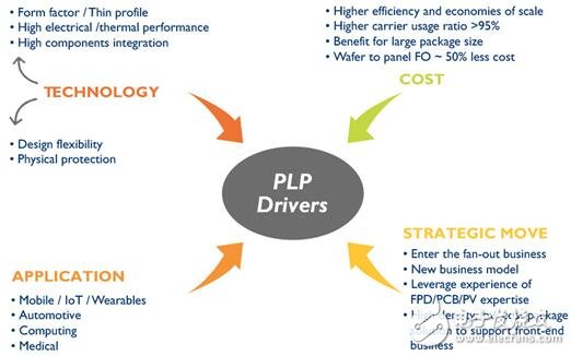
Market drivers for board-level packaging platforms
Supply chain status
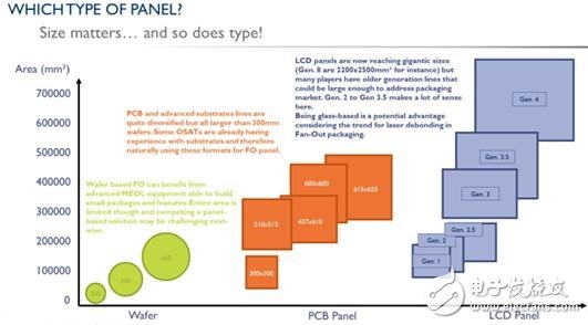
Many package platforms can be considered panel-based packages, however, this report only classifies the two types of package technologies as PLPs, which are manufactured using RDL interconnects, and further at the panel level (panel size >300 mm x 300 mm) Assembled: FOPLP and embedded chips. Among them, FOPLP has attracted more attention from many manufacturers (including equipment manufacturers and suppliers), so this report focuses on FOPLP and conducts more in-depth research and analysis on FOPLP.
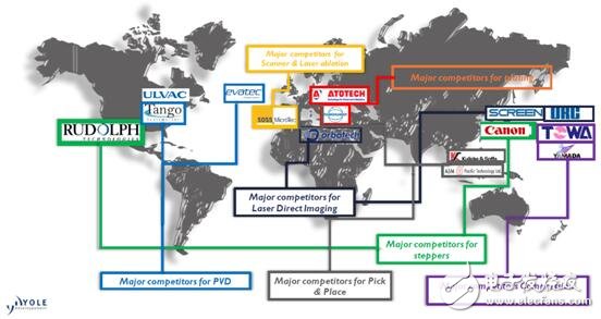
PLP Equipment Supplier Overview
Many manufacturers have developed their own FOPLP technology, but after years of development / verification / sampling, only three manufacturers will finally enter mass production in 2018, they are: Powertech Technologies (PTI), NEPES and SEMCO. NEPES has started small-scale production in 2017. The ASE, which is partnered with Deca Technologies, is also in an advanced stage of development and will be commercially available in 2019 or 2020. Each vendor has its own business strategy to develop its own FOPLP technology (different panel sizes, different infrastructure, etc.).
For example, NEPES focuses on extensive design (>10/10 L/S), and target applications include automotive, sensors, and the Internet of Things, and it is likely that high-density designs will not be developed. On the other hand, the long-term goals of PTI and SEMCO refer to mid- to high-end applications requiring L/S of 8/8 or less. At the same time, Unimicron is developing a business model to manufacture high-density RDLs themselves, and further assembly is done by OSAT partners or customers. In addition, major OSAT vendors such as Amkor and JCET/STATS ChipPAC are currently in the stage of “waiting for change†to evaluate multiple options, which are not expected until 2022. Enter mass production.
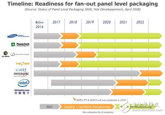
The main manufacturer's preparation timeline for fan-out board-level packaging
For PLP, the device is no longer a bottleneck. The organic platform is also available on the market to support various processes in board-level packaging. However, some machines that support high-density board-level packaging are special and expensive. Therefore, the bottleneck lies in the cost of the machine and whether it can be bought. For some panel manufacturing processes (electroplating, physical vapor deposition PVD, molding, die attach and dicing, etc.), it has been available for use in the PCB, flat panel display or LCD industry. However, for the key process steps inherent in other advanced packages (such as lithography), new and upgraded machine processing capabilities are needed to support these processes, such as fine L/S patterning on the panel, thick lithography, and panels. Processing capacity, exposure field size, and depth of focus. Equipment suppliers have been working on these machines for the past few years.
Equipment vendors are adopting different strategies to enter the PLP business: M&A (for example, Rudolph Technologies developed a PLP-based machine based on technology acquired from the acquisition of AZORES flat panel display panel printing equipment); using machines from other businesses Experience and upgrade (eg Evatech, Atotech, SCREEN); organically develop PLP machine (ASM) from 0. In addition, some machine suppliers with strong market positions in the FOWLP market are still skeptical about the PLP business and are therefore still waiting to see (eg Ultratech, Applied Materials, Lam Research).
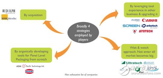
Strategy for machine supplier to enter board-level packaging business
Board-level packaging technical challenges and scale manufacturing roadmap
The widespread use of FOPLP requires progressively meeting certain criteria and overcoming some of the challenges. These standards/challenges mean a large amount of capital investment, standardization, multi-source availability and, most importantly, market availability to ensure the continued operation of the panel production line. There are also technical challenges on large-sized panels, such as warpage control, chip placement accuracy, and manufacturing below 10/10um line width.
Technical challenges faced by FOPLP scale applications
Standardization of panel dimensions and assembly processes is the biggest obstacle to FOPLP applications. Various manufacturers are using different panel sizes and infrastructure (PCB / LCD / WLP / PV / Mix) to develop their own processes to meet the needs of specific applications and customers. In this context, it is difficult for end users to achieve multi-source procurement. In addition, it is difficult for equipment suppliers to design and manufacture equipment according to the requirements of different customers.
Given the adverse effects of these technical challenges on yield, FOPLP entering mass production will support a relatively simple design: >10/10 umL/S, 15 x 15mm2 package size, and multi-chip SiP integration.

Fan-out board-level package mass production roadmap
Some companies involved in the report: AMS, Amicra Microtechnologies, Amkor, Analog Devices, Apple, Applied Materials, Asahi Kasei, ASE, ASM Pacific, AT&S, Atotech, AVX, Besi, Bosch, Canon, CEA-LETI, Continental, Dai Nippon , Daimler, DNP, DYCONEX AG, Dow Electronic Materials, Evatech, EVG Group, Ford, Fujikura, GaN Systems, General Electric, Hanmi, HD Micro/DuPont, Heidelberg Instruments, HighTec EDV System, Huawei, Ibiden, Infineon, Intel, IPDiA , IME A*Star, IMEC, ITRI, IZM Fraunhofer, J-Devices, JSR Micro, Kulicke & Soffa (K&S), Kyocera, Maxim, Merck/AZ EM, Mitsui Kinzoku, Murata Electronics, Nagase, Nanium, NCAP China, Nikon , Nitto Denko, ON Semiconductor, Orbotech, ORC, Panasonic, Powertech Technologies, Qorvo, Qualcomm, Rohm Semiconductor, Rudolph, Sarda Technologies, Schweizer, SCREEN, Shinko, Shin Etsu, STMicroelectronics, SUSS MicroTec, Taiyo Yuden, Tazmo, TCL, TDK -EPCOS, TEL, Texas Instruments (TI), Thales, Towa, TransSiP, Tokyo Ohka Kogyo Co., LTD. (TOK), TSMC, Shin-Etsu MicroSi, Samsun g Electro Mechanics (SEMCO), STATS ChipPAC, Ultratech, Unimicron, USHIO, UTAC, Valeo, Vishay, Yamada...
Dongguan SOLEPIN Electronics Co., Ltd , https://www.wentae.com