How to popularize FPGA resources? New transformation of Alibaba Cloud
FPGA (Field Programmable Gate Array), because of its hardware parallel acceleration capability and programmable features, shines in the traditional communication field and IC design field. Along the way, FPGA is not an emerging hardware device. Due to its high development threshold, the requirements for the release and deployment of hardware acceleration algorithms are very high. The use of FPGA has always been a cold beauty, and it has not entered the home of ordinary people, resulting in FPGA The computing potential has not yet been fully tapped.
Next, let's take a look at how Alibaba Cloud has transformed it.
Alibaba Cloud ECS's heterogeneous computing team and high-performance computing team have been committed to "civilization" of computing resources; the E-HPC that the high-performance computing team is doing is to enable all users on the cloud to instantly have a small supercomputer Clustering makes supercomputing no longer just the privilege of some supercomputing centers and universities; and our heterogeneous computing team is committed to providing users with the fastest and latest computing equipment on the cloud to make the once-cold computing resources It is no longer a thousand miles away: we launched the FaaS service of the FPGA cloud server. The F1 and F2 instances have provided external services, and the small-size device computing power of Intel and Xilinx can be given to customers through one-click deployment.
Today we are pleased to announce that the newly-enlarged large-scale FPGA instance, a heterogeneous computing instance F3 based on Xilinx 16nm Virtex UltraScale + device VU9P, is online on Alibaba Cloud!
We take this opportunity to make a technical interpretation of the Alibaba Cloud FPGA computing service (hereinafter referred to as FaaS) itself, as well as the underlying hardware architecture and platform architecture of the F3 instance released this time.
FaaS
Ali FPGA cloud server platform FaaS (FPGA as a Service) provides a unified hardware platform and middleware in the cloud, which can greatly reduce the development and deployment costs of accelerators. Accelerator developers' accelerators can form services to accelerator users and eliminate the hardware barriers between acceleration technology and end users. Users can use acceleration services directly on demand without knowing the underlying hardware.
In order to provide accelerator providers and consumers with a more efficient and unified development and deployment platform, FaaS provides two major packages: HDK and SDK.
HDK
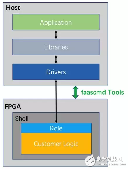
HDK provides a unified FPGA hardware interface to all accelerator developers, helping users solve the most difficult high-speed interface development and debugging in FPGA development in advance, such as PCIe, SERDES interface, DDR controller, etc .; so that users can directly get the hardware platform The maximum performance of the interface with the FPGA will not cause the hardware platform performance to be wasted due to the lack of team development capabilities and experience; the efficient, reliable, and unified interface suite also provides security for the platform on the cloud, and the device stability is guaranteed. User interface design problems cause server downtime; at the same time, it can prevent users from illegally operating the host on the FPGA side to provide security for the entire cloud.
HDK includes two parts, Shell and Role; Shell is deployed in a static area and provides the above-mentioned unified interface part.
Under the premise of providing unified interface, security and convenience, Alibaba Cloud FaaS HDK also makes its best efforts to ensure the flexibility of user design, and the concept of Role came into being. Role is deployed in the dynamic area and is developed and provided in advance outside the Shell, and users can use it with Customer Logic. Unlike Shell, users can replace the Role part at any time according to their needs; this combination of Shell + Role ensures the lightest weight and stability of Shell, while taking into account the unity, convenience and flexibility.
SDK
The SDK includes two parts:
Host-side drivers (Drivers) and software libraries (Libraries) corresponding to HDK (Shell + Role)
FPGA management tool faascmd kit
The driver and software library correspond to Shell and Role of HDK. Together with HDK, it provides users with unified and flexible software support, such as DMA driver, register access driver and so on.
The faascmd tool suite provides users with FPGA management services on the cloud, including security verification, FPGA image generation, download and management, FPGA accelerator card status query feedback and other functions. The use of FPGA in the public environment needs to consider the security of the user's FPGA file. The secret key provided by faascmd and the OSS bucket designation mechanism effectively ensure the privacy of the user's FPGA download file. In offline development and applications, developers directly download FPGAs, but in the cloud environment, users directly operate on public FPGA resources and have a greater impact on security. The Faascmd tool will isolate user operation applications and physical FPGA resources to ensure user download safety and provide users with an offline operation-like experience; at the same time, it will verify the netlist submitted by users to improve safety and reduce risks. Faascmd also provides a calling interface, users can easily call management tools in their own apps, combined with their own accelerator features to achieve various management functions.
FaaS's IP market
FaaS reduces the barriers to entry for FPGA developers: FPGA resources on the cloud and flexible payment models make hardware resources within reach; at the same time, the development process is simplified, the development interface is unified, and the core acceleration logic is removed from the surrounding The isolation of hardware device interface debugging allows emerging applications of FPGAs to focus only on the core logic of business acceleration and iterate quickly; on these two points, Alibaba Cloud ’s FaaS has taken the first step towards civilianization of FPGA computing resources.
But even if it greatly simplifies the development process and provides hardware resources within reach, FPGAs still have a certain development threshold. How to maximize the value of existing FPGA logic IP, and connect the demand side and provider side of FPGA acceleration to expand the ecology? The important point is how to solve the problem of ensuring FPGA acceleration IP security at the public cloud data center level, especially the output and deployment of untrusted third parties. How does FaaS solve this problem?
The answer is through the Alibaba Cloud FaaS IP market. Technically, the customized virtualization technology jointly developed with Xilinx achieves strong isolation between IP acceleration and deployment environment. IP users are completely isolated from IP netlist files. Netlist file transmission, deployment, and acceleration processes are not affected by users throughout the process. It can be seen that at the same time, the accelerated computing power can be transparently opened to third-party users using the IP. This is another technological innovation of Alibaba Cloud's accelerated service on the FPGA cloud. This innovation completely eliminates the possibility of FPGA IP being pirated when output on the cloud, and provides a very high security protection mechanism.
A stricter confidentiality mechanism is also being planned: IP can be encrypted and protected by Alibaba Cloud ’s KMS encryption service soon. Every time the IP is loaded, it is necessary to obtain the key decryption from the KMS service, so as to download for the use of IP It is well documented; and makes the IP of the IP issuer safe in the data center, because without the KMS key of the IP provider, even Alibaba Cloud cannot decrypt the encrypted netlist.
With the help of Alibaba Cloud FaaS IP market, even users who have never had any FPGA development experience can get the corresponding acceleration logic from the IP market with one click and quickly deploy it to the corresponding FPGA device. We believe that through out-of-the-box hardware resources, unified software and hardware logic development interfaces, and the IP market, Alibaba Cloud can truly fulfill its commitment to civilianization of FPGA computing resources.
F3 hardware architecture
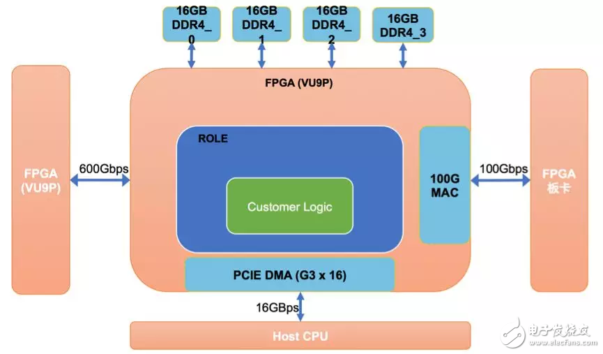
Alibaba Cloud FaaS 'F3 instance is based on the underlying hardware and is a VU9P board that uses high-performance single-card dual-chip independently developed by Alibaba Cloud. The key point here is: single card dual chip. Some users must ask why this design? What are the advantages of single-card dual-chip hardware design?
First of all, for users, through the specification design of single card and two chips, together with the self-developed server supporting Alibaba Cloud, it can provide up to 16 VU9P calculation instances for a single instance. 16 VU9P is very high computing density, which is the first purpose of designing a single card dual chip: by increasing the computing density, more acceleration chips are integrated under the same computing unit, which can effectively reduce the cost of unit computing power , From the significant cost reduction and the vertical computing power of unit instances, customers can benefit from both.
Two VU9P chips with a single card and two chips are connected to the system through a PCIe bridge. What about the communication between the two chips? Is it only possible to use the PCIe bus? The answer is no. In addition to FPGA Direct's ability to communicate with each other through PCIe, there are special considerations on Alibaba Cloud's self-developed boards. Between the two chips, we designed a high-speed interconnection channel, so that two FPGAs can communicate at a rate of up to 600Gb / s through this special channel. This communication technology is called FPGA Link. You should know that the access switch optical port communication currently deployed in the mainstream of data centers can only reach the communication rate of 100Gb / s, and the higher 200Gb / s switch is still in trial deployment.
Imagine that without additional switches and optical port hardware, the two FPGA chips can communicate through FPGA Link technology with ultra-short delay at 6 times the rate of mainstream optical port communication. This will help users to open a large number at a very low cost. New FPGA accelerated application mode. For example, when small-scale chip simulation requires two devices to be deployed, the overall simulation module can be disassembled and deployed on two chips. The data path and synchronization signal between the two chips are interconnected through a high-speed channel; There are other application scenarios where functional modules need to be deployed on two FPGA chips, and a large amount of data exchange is required between the two, such as video transcoding scenarios: a small-scale decoding unit with a large number of modules, video The processing unit is deployed on an FPGA, and the coding unit with a larger area is placed on another FPGA, and the codec modules exchange high-speed interconnection to exchange bare video streams. This will greatly improve the difficulty of deployment and greatly decouple the interdependence and design difficulty between the two modules. The above mentioned two examples, readers must be able to think in reverse, for other scenarios that require pipeline processing and require a large amount of data exchange, the dual-chip instance of Alibaba Cloud ’s F3 instance can provide customers with the greatest value.
Many application scenarios have requirements for onboard DDR storage. Alibaba Cloud's F3 example is equipped with 64GB of DDR memory visible to customers for each FPGA. The 64GB of DDR is divided into 4 channels, which are connected to the three silicon units of VU9P. One channel corresponds to the 16GB DDR reserved for resident The 48GB storage corresponding to the remaining 3 channels can be loaded and used by customer logic in an optional manner.
At present, we have seen the dual-chip instance. In addition to the FPGA Direct technology and the high-speed interconnect capability of FPGA Link up to 600Gb / s, it is also worth mentioning that the dual-chip instance and other dual-chip instance boards can also pass The 400Gb / s optical port is interconnected, and the 400Gb / s Ethernet protocol driver is accelerated by the MAC hard core preset by Xilinx without occupying logical area; through Ethernet or a custom lightweight communication protocol, it can be used in 16 chips Between, and more chips to build 2D Mesh or ring interconnection, to further expand the use mode and application scenarios of multi-chip interconnection.
Finally, the previous picture gives everyone a more specific understanding of the technical analysis of the hardware done above:
F3 logical structure
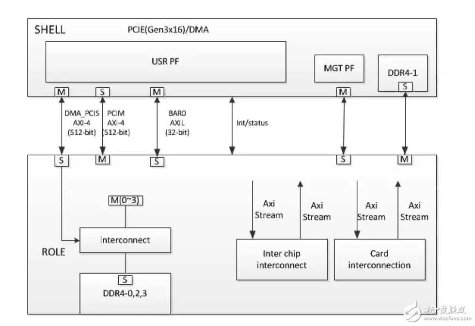
F3 logical structure, before technical analysis, first give you a logical architecture diagram:
SHELL and ROLE concepts
★ SHELL:
Shell is the static area of ​​FPGA, which contains user PCIe, management PCIEe, board management system and a DDR access channel. In order to improve the security and stability of the board, the user has no right to modify the SHELL area.
★ ROLE:
We put forward the concept of Role in the design. Role and Shell are similar packages. Role and Custom Logic are in the dynamic area. The proposal of Role allows us to make Shell more lightweight. We have implemented the same Shell through Role, which can support both OpenCL development and RTL development. Finally, Role's abstraction again lowers the development threshold for FPGAs. We provide basic Roles, and also allow users to design Roles themselves. We hope that more third-party designers will make their FaaS platform more exciting by sharing their Role.
Introduction to ROLE internal structure
Interconnect: This part mainly provides users with access to four DDR channels and USER_PCIe access to four DDR channels. This module helps users isolate the clock domain, allowing user logic to access 4 DDR channels on the same clock domain.
Inter chip interconnect: FPGA single card dual chip interconnection path;
Card interconnect: interconnection path between FPGA cards;
Custom Logic: User-defined logic part;
Introduction to Custom Logic
User logic is part of Role and belongs to the dynamic loading area. In order to facilitate users' standardized use, we used standard AXI-4 and AXI-LITE interfaces in RTL design.
1. We will introduce the user interface in detail, the list is as follows:
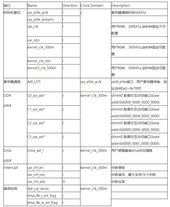
Note: The inter-board interconnection and the Kaka interconnection interface are not provided by default during the invitation test phase. Special applications are required to open to the outside world.
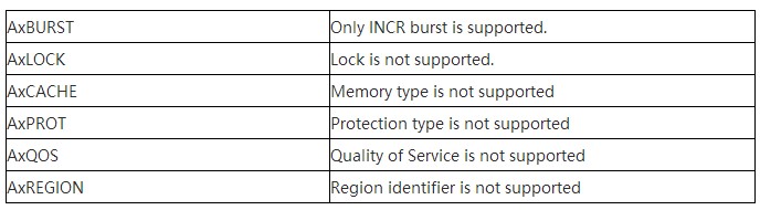
2. AXI-4 and AXI-Lite limitations
3. As we mentioned in the introduction to Role, users can customize Role operations. In order to facilitate users to use the platform more efficiently, our Alibaba Cloud FaaS team is releasing multiple Role versions. Please stay tuned. It is always our mission to lower the threshold for user use, shorten development time, and improve the FPGA usage ecology.
Solar On and Off Grid Inverter
Grid Tie Inverter,Solar Pump Inverter,On Grid Solar Inverter,On And Off Grid Inverter
Jinan Xinyuhua Energy Technology Co.,Ltd , https://www.xyhenergy.com