In-depth analysis of SK Hynix's latest 72-layer 3D NAND
[In-depth analysis of SK Hynix's latest 72-layer 3D NAND] In SKHynix's 72-layer (72L) TLCNAND flash memory, the so-called P-BiCS (Pipe-shaped BitCostScalable) cell uses a pipeline gate to link each NAND character. NAND string; from its layout, the chip contains four planes and two-sided wordline switches/decoders.
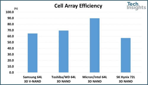
The efficiency of the memory array is about 57% because of relatively large memory and other peripherals; and the efficiency of the memory arrays of the 36L and 48L products of SKHynix is ​​67.5% and 64.0%, respectively. This trend shows that SKHynix should develop smaller-size designs for next-generation chips.
The 64L3DTLCNANS die of Samsung and Toshiba/WD (Toshiba/Western Digital) has more than 65% memory array efficiency; however, the above memory chip sizes and functions are similar.
Comparing Efficiency of 64L and 72L 3D NAND Flash Cell Arrays (Source: TechInsights)
SKHynix72LNAND flash memory has a bit density of 3.55Gbits/mm2, which is higher than that of Samsung/WD's 64L chip, while Micron/Intel's 64L3DNAND chip has the highest bit density among the four solutions, mainly because of the use of the name CuA. (CMOS underthearray) unique brick layout.
Bit density comparison of 64L and 72L 3D NAND memory chips (Source: TechInsights)
In the 3D NAND memory cell architecture, the SKHynix chip stacks a total of 82 gates, including selectors and dummy word lines (DWL); we know that 72 gates are used for active word line cells, and most The top three gates are the selector gates (SG) for the source and drain, and the remaining 7 gates are for DWL and isolation gates.
In the 64L NAND components of various manufacturers we see:
• Samsung employs a total of 71 gates, of which 3 are for SG and 4 for DWL;
• The total number of gates for Toshiba/WD products is 73, of which 7 are for SG and 2 for DWL;
• The total number of gates for Micron/Intel products is 76, of which 2 are for SG and 7 for DWL.
The vertical cell efficiency calculation method is the number of active word lines divided by the total number of vertical stack gates; the result is the process efficiency of the 3D NAND memory cell architecture. The vertical unit efficiency of the SKHynix72L product is 87.8%, and that of the Toshiba/WD's 64LBiCS product. Samsung's 64L product efficiency is 90.1%, while the Micron/Intel's 64L product efficiency is 84.2%, as shown in the figure below.
Vertical Unit Efficiency of 64L and 72L 3D NAND Memory Products (Source: TechInsights)
SKHynix's previous 36L and 48L products use a single-step etching process to create channel holes that are 43 and 55 gates in total; a new generation of 72L memory cells uses a two-step etching process to create access to Holes. On the pipeline gate, the lower 42 gates and the upper 40 gates are respectively formed in two different etching steps. The slits and sub-slits are formed by single-step etching. The process integration process is as follows:
Pipeline gate molding (lower part)
Channel etching (lower part)
The sacrificial layer is filled with holes;
Mold forming (upper part);
Channel etching (upper part);
Sacrificial layer removal;
Channel forming.
Micron/Intel's 64L product uses a dual-stack NAND string architecture with a plate between the upper and lower stacks; SKHynix's 72L product uses a two-step etching process instead of a dual-stack NAND string, engineer The process steps must be tightly controlled to avoid misalignment of the channel holes in the upper and lower parts; the size of the hole is only about 10 nm in the 256Gbit 72L product.
Geekvape Vape,Geek Bar Disposable Vape,Geek Bar Vape Kit,Geek Bar Vape Pod
TSVAPE Wholesale/OEM/ODM , https://www.tsvaping.com