Development and Research of FPGA Video System Based on AXI4Stream Bus
Abstract: Based on the AXI4Stream bus protocol, a video system with defective pixel correction, color filter array interpolation, image denoising real-time image acquisition and display function is implemented on the FPGA provided by Xilinx. The AXI4Stream bus protocol was proposed by ARM, which is designed for on-chip communication of video, audio, array and other data. The use of IP cores for embedded system development has obvious advantages such as simplified design and shortened development cycle. The design results show that the video system based on AXI4Stream bus has the advantages of versatility, independence, simplicity and easy maintenance.
Introduction With the development of technology, real-time video processing technology has received widespread research attention as one of the most active research directions in the field of digital signal processing, and is widely used in communications, aerospace, radar, telemetry, remote sensing and multimedia industries. Compared with the mode of constructing circuits with separate components, the new video acquisition system based on field programmable gate array (FPGA) technology has obvious advantages in processing speed, reliability, cost, expansion capability and development cycle.
In recent years, FPGA-based video capture systems have been fully studied [1, 2, 3, 4], but in view of the fact that such research does not perform general format processing on image data, the system is too integrated, and modules are too dependent on each other. System versatility. AXI (Advanced eXtensible Interface) is a bus protocol, which is an important part of ARM's AMBA (Advanced Microcontroller Bust Architecutre) protocol. It is an on-chip bus for high performance, high bandwidth and low latency. AXI4 was released by ARM in 2010, and AXI4Stream is a subclass of AXI4, which is especially suitable for the transmission of streaming media data [5]. In this paper, the entire video acquisition system is re-examined with a bus dedicated to video data transmission, namely AXI4Stream bus. In the case of ensuring high integration, the versatility of the system is greatly improved by simplifying the inter-module communication interface, and has good practicability and scalability.
The AXI4Stream bus is mainly used in systems where digital information is transmitted in one direction. The sampled physical quantities, such as image pixel point data, audio sample data, and data processed by discrete digital signal systems, are particularly suitable for this bus protocol. AXI4Stream is a one-way bus that transfers data based on handshake signals from the master to the slave. The AXI4Stream bus used in the system is based on the AMBA4 AXI4Stream Protocol v1.0 reference manual [6] released by ARM, which has been widely used in embedded systems in the mainstream market. In the case of ensuring complete functions, the design uses only part of the signal line for data transmission. Related signal line name and function explanation diagram - editor's note.
2 Introduction to system structureThe system is based on AXIStream bus, with FPGA as the main control chip. DDR2 caches image data, reads data from CMOS image sensor and processes it, then sends it into video encoding chip, and finally outputs it through DVI interface, realizing a real-time image acquisition and display. Video system. The hardware block diagram of the system is shown in Figure 1.
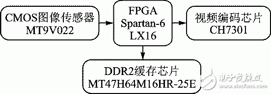
Figure 1 system hardware block diagram
The system selects the chipset: CMOS image sensor selects ApTIna MT9V022, the effective resolution is 752H & TImes; 481V, the chip is widely used in video surveillance, machine vision and other systems; FPGA main control chip selects Xilinx Spartan6LX16, the chip Using 45 nm low-power process technology, providing up to 15 000 logic cells, meeting the market requirements of low-cost, high-capacity applications, and greatly reducing the total power consumption; DDR cache chip selects MT47H64M16HR25E provided by Micro, storage The capacity is 1 Gb; the video encoding chip uses the CH7301 chip provided by Chrontel, which has been widely used in display interface circuits.
Since the main control chip uses an FPGA manufactured by Xilinx, the development software uses the ISE (Integrated Software Environment) Design Suit kit provided by the company.
The structure of the system function module is shown in Figure 2. All modules are implemented in ISE using the hardware description language Verilog HDL.
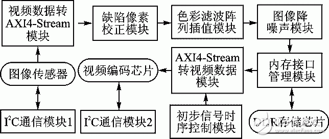
Figure 2 System function block structure block diagram
The following points are mainly considered for the functional modules shown in Figure 1:
1 The CMOS image sensor chip and the video encoding chip communicate with the main control FPGA chip using the I2C protocol, so a special I2C communication module is added.
2 The image data sent by the CMOS image sensor is not based on the AXI4Stream bus. A universal video data is transferred to the AXI4Stream module for AXI4Stream formatting of the data.
3 The image sensor has a defective pixel (DefecTIve Pixel), which needs to be removed by the algorithm, so the data needs to be processed by the DefecTIve Pixel Correction module.
4 The pixel data obtained from the image sensor is Bayer format (Bayer Patten), which needs to be converted to RGB format, and the Color Filter Array Interpolation module is introduced.
5 After the format conversion, the original data has more noise, and it is necessary to introduce an Image Noise Reduction module.
6 The amount of image data is huge, and the limited storage space of the FPGA cannot meet the data throughput requirements. In order to solve this problem, the external memory chip DDR2 is introduced and managed by a dedicated Memory Interface Controller module.
7 Image data needs to match the corresponding timing signals for output, so a video timing controller (Video Timing Controller) module is designed to solve this problem.
8 The data format of the video encoding chip is based on the AXI4Stream protocol. It is necessary to introduce the AXI4Stream to video data module to integrate the image data and video timing control signals into a data format that can be directly utilized by the encoding chip.
3.1 I2C bus communication module
The I2C bus protocol has the following different transmission codes, in order: start bit, slave device address, acknowledge bit, data message, and stop bit. (stop bit). A typical I2C bus read and write timing is shown in Figure 3. SCK is the clock signal line and SDA is the data signal line. In the idle state, both SCK and SDA are high. The read/write start flag is that the SDA signal line is pulled low to generate a start bit, and then the master device sends an 8-bit slave address signal. The last bit of the device address determines the read and write nature of the operation. A low level indicates a write operation and a high level indicates a read operation. The slave then pulls the SDA signal line low to answer. The master device then performs a read or write operation in units of 8 bits, and after the response, pulls up the SDA signal line to indicate the stop bit and returns to the idle state.
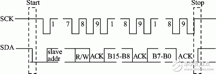
Figure 3 I2C bus timing transfer diagram
3.2 Video data to AXI4Stream module The timing output by the CMOS image sensor MT9V022 is shown in Figure 4, where LINE_VALID indicates that the row data is valid, and FRAME_VALID indicates that the frame data is valid. The module detects the start and end of each line of data in the image by detecting the rising and falling edges of the FRAME_VALID and LINE_VALID signals, and matches the AXI4Stream interface signals by combining the 10-bit pixel information transmitted in parallel. The module outputs in a master mode interface. The interface signals include: tdata for pixel point data; TVALID and tready for handshake signals; tuser for the first pixel of the first line of a frame image; tlast for the last pixel of each line point.
The functional simulation of this module in the ModelSim software - editor's note. The module has been verified to implement data format conversion.
3.3 Defective Pixel Correction Module There is a certain amount of defective pixel data in the data acquired from the image sensor due to manufacturing defects, failures in daily operations, or changes in pixel voltage due to temperature or exposure differences. The characteristics of these defective pixels can be summarized as follows: inactivation (total low), active (total high), adhesion (fixed value). These anomalies can be further characterized as static (always existing) or dynamic (as a function of exposure or temperature).
The core code of the module uses the IP core provided by Xilinx, Defective Pixel Correction IP Core [7]. The programming interface is shown in Figure 5.
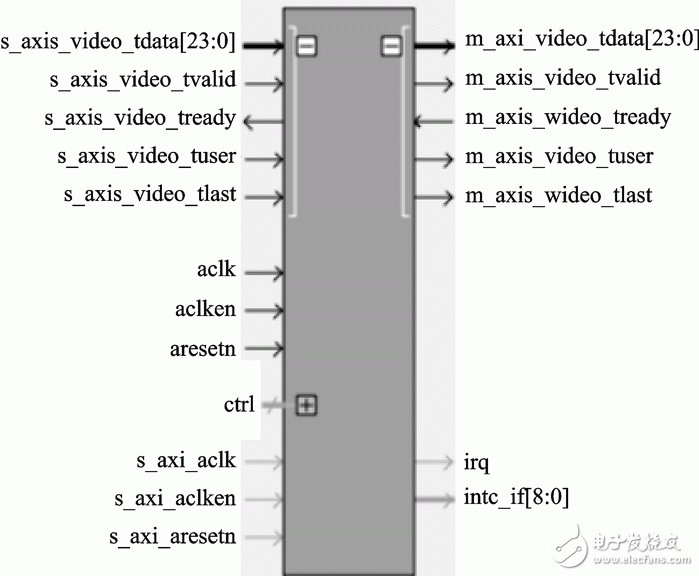
Figure 5 Defective pixel correction module programming interface
For larger fixed areas in the image, the module needs to determine whether the area is still or singular, that is, defective pixels. Since the processed data is in the original Bayer format, this module will track and match the pixels of a pixel adjacent and in the same format (for example, the same green component), and record the information between the pixels whose difference exceeds the threshold. Come down.
The threshold value and the number of consecutive comparison frames are preset in the module, and when the pixel difference exceeds a predetermined threshold in consecutive frames, it can be determined as a defective pixel. For defective pixels, the module replaces adjacent format pixel data by interpolation.
The wire harness simplifies the building of these larger components by integrating the wiring into a single unit, or several units, for [drop-in" installation. By binding the many wires, cables, and subassemblies into a harness, the OEM or installer only has one component to install. In addition, a wire harness allows the completed assembly to be better secured against the effects of abrasion and vibration, and by constricting the wires into a non-flexing bundle, usage of space is optimized.
Game Machine Wire Assembly, wire harness for gaming machine, electrical wire assembly, gaming wire harnesses
ETOP WIREHARNESS LIMITED , https://www.wireharness-assembling.com