Bioelectric signal acquisition scheme based on IMEC
This article introduces the SiC technology using IMEC. Its development focus is to further reduce the size of the integrated EEG system and integrate low-power processing technology, wireless communication technology and energy extraction technology. Add a solar cell and The additional stacked layers of the energy storage circuit can form a completely independent bioelectric signal acquisition scheme.
The wireless bioelectronic communication system will greatly improve people's quality of life in the future. To realize this ideal, it is necessary to develop a body-area networks (BAN) composed of small intelligent sensor nodes. The sensor node is used to collect important information of the human body, and then send the information to a central intelligent node, and then the intelligent node sends the information to the base station through wireless communication. These sensor nodes can be designed and implemented using 3-D stack-based (System-in-a-cube, SiC) integration technology.
The small low-power sensor / actuator nodes used to form the body area network must have sufficient computing power and wireless communication capabilities, and the antenna should be integrated. The intelligence of each node must enable it to complete the tasks assigned to it, such as data storage and algorithm implementation, and even complete complex nonlinear data analysis. In addition, they should be able to communicate with other sensor nodes or central nodes worn on the body. The central node communicates with the outside world through standard telecommunications facilities such as wireless local area networks or cellular telephone networks. Such a BAN can provide services for individuals, including the supervision and treatment of chronic diseases, medical diagnosis, home monitoring, biometrics, and exercise and health tracking.
IMEC has recently achieved a technological breakthrough and developed a small three-dimensional stacked SiC system with a volume of only 1 cm3. The first 3-D stacked prototype includes a commercial low-power microcontroller with 8 million instructions per second, a 2.4GHz wireless transceiver, several crystal oscillators and other necessary passive devices, as well as a user Design a monopole antenna for the matching network. Among them, the microcontroller and wireless transceiver have adopted the most advanced energy-saving technology. The high integration of the system is achieved by stacking multiple layers with different functions along the Z axis through a technique called "3-D stacking". Each layer is connected to the adjacent layer by double-row macro solder balls.
Using this general stacking technology can achieve any kind of module combination. This low-power 3-D SiC system can be used in a variety of wireless products, from the monitoring of human body information (brain activity, muscle activity, and heartbeat) to the monitoring of environmental data (temperature, pressure, and humidity), which are ultimately used to form a BAN. Due to its unique stacking characteristics, this technology can even integrate a specific sensor into a single layer to form a dedicated cubic sensor module.
The development of SiC is part of IMEC's ​​Human ++ plan. It is envisioned that multiple similar SiC sensor nodes will be combined to form a BAN. The Human ++ project combines wireless communication technology, packaging technology, energy extraction technology and low-power design technology, with the goal of developing devices that can improve people's quality of life.
Whether this kind of BAN can be successfully achieved depends on the degree of expansion of our existing device capabilities. Therefore, we must first remove several obstacles in medicine and technology. First, the battery-powered equipment used today has a limited lifespan and must be managed to extend its lifespan. Second, the interaction between the sensor and the actuator should also be amplified in order to adapt to the needs of new applications such as the measurement of multiple physiological parameters. Third, the device should possess certain intelligence, be able to store, process and transmit data. In addition, the functions of the device must be expanded to enable chemical and biological measurements. Finally, there should be a thorough understanding of medical phenomena. 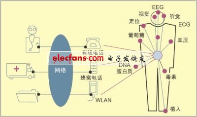
Figure 1: IMEC's ​​2010 technology outlook
Rich experience and proprietary technology have made IMEC achieve new breakthroughs in multiple technical fields, which creates opportunities for responding to such challenges. Semiconductor calibration technology has spawned electronic devices with smaller size and lower power consumption, making it possible to develop more powerful therapeutic and diagnostic devices.
With the development of microsystem technology, especially microelectromechanical system (MEMS) technology, devices with both electronic and mechanical characteristics have been produced. The first application of MEMS technology is to develop energy absorbers that power autonomous medical systems, such as those based on the conversion of thermal energy to electrical energy, which can use body heat to generate micro-energy. The source of this energy is endless, so the system can keep working all the time, and the life span is almost infinite. But the question is how to prove that this device can extract enough energy from the human body (that is, at least 100 milliwatts) to support the operation of future systems. Another possible application of MEMS technology is in sensor and actuator systems. These systems are used to provide an interface with the outside world and mixed signal circuits around it. Finally, the use of MEMS technology can also develop new components (such as resonators) that can be used in ultra-low power (ULP) RF transceivers. ULP radio frequency devices can be used to communicate between sensor nodes and wearable central nodes, with an average power consumption of 50 μW.
Due to the use of new packaging technology, a large number of different types of complex systems (such as fluid biosensors, radio frequency transceivers, microprocessors, and batteries) can be integrated into a very small device, making mobile wireless medical devices more wearable Simple.
Nanotechnology makes it possible to use small interconnected devices to achieve direct interactions between body biological systems such as cells, antibodies, or DNA. Both new biosensors and transplants may use this technology.
If a low-power processor structure can be developed, the intelligence of the sensor node will be further increased, so that the sensor itself can perform more complicated data processing. This requires us to design a ULP processor structure (dedicated instruction set processor structure and data memory structure) that can run biomedical applications. Today's biomedical applications generally require 20 million per second on non-optimized processors. To 1 billion operations.
Finally, the use of new design techniques can effectively model, simulate, and design the above applications.
Although the dream of human wearing BAN became reality as early as 2010, some related technologies have emerged, the most famous of which is its application in the field of bioelectronics research. Bioelectronics is an area containing unlimited opportunities. The combination of biological (or biochemical) reactions and electronic signal detection and amplification has produced new exciting bioelectronic diagnostics. Similarly, the use of neural networks and computer chips on the micro level can also develop pharmacological sensors, and even design neuroelectric processors for medical and technical applications.
Using IMEC's ​​SiC technology, the wireless EEG system can be integrated into a device with a volume of only 1 cm3. In this way, the patient can wear a very comfortable wireless EEG device for EEG. IMEC's ​​future development focus is to further reduce the size of the integrated EEG system and integrate its low-power processing technology, wireless communication technology, and energy extraction technology. Adding an additional stacked layer with solar cells and energy storage circuits to the existing system may form a completely independent solution.
Indoor Fixed Advertising Led Screen
Indoor fixed advertising LED screens are large electronic display screens that are used for advertising purposes indoors. These screens are typically installed in high-traffic areas such as shopping malls, airports, train stations, and other public spaces.
Hot-selling series are p2/p2.5/p4/p5 led display video wall.
Indoor Fixed Advertising Led Screen,Indoor Led Wall Billboards,Indoor Fixed Led Billboards,Shopping Mall Led Display
Guangzhou Cheng Wen Photoelectric Technology Co., Ltd. , https://www.cwledwall.com