Power switch design that meets USB specifications
1 Introduction
Universal Serial Bus (Universal Serial Bus) makes the connection between PC and external devices simple and fast. With the development of computers and USB-related portable devices, USB will be more widely used. Due to the plug-and-play characteristics of USB, the power switch can flow a few amps of current at the moment of abnormal load, causing damage to the circuit.
The USB power switch designed in this paper uses a bootstrap charge pump to provide 2 times the gate drive voltage of the power supply for the N-type power transistor. In the event of an abnormal load, the overcurrent protection circuit can quickly limit the power tube current to avoid damage to the circuit caused by hot swap.
2 USB switch circuit overall design ideas
Figure 1 shows the overall design of the USB power switch. Among them, VIN is the power input, and VOUT is the USB output. Under normal load conditions, a sufficiently high gate drive voltage is generated by the charge pump to operate NHV1 in the deep linear region to reduce conduction losses from the input supply (VIN) to the load voltage (VOUT). When the power tube current is higher than 1A, Currentsense outputs a high level to the overcurrent protection circuit (Currentlimit); the overcurrent protection circuit adjusts the charge pump output (VPUMP) by feeding back the load voltage to the charge pump, thereby making the power tube work state. From the linear region to the saturation region, the power tube current is limited to achieve the purpose of protecting the power tube. When the load returns to normal, the Currentsense output is low and the charge pump works normally.
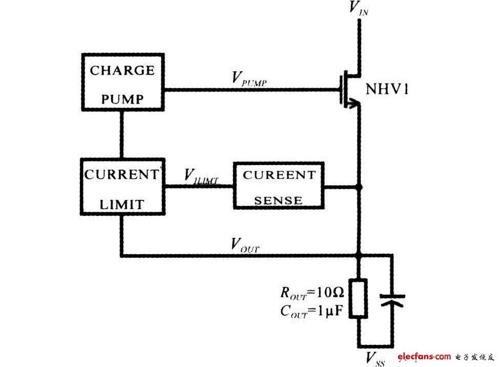
Figure 1 USB power switch schematic
3 charge pump design
2 is a circuit schematic diagram of a bootstrap type (SelfBooST) charge pump. In the figure, the clock signal is used to control the charge pump operation. In the initial stage, the charge on C1 and the power gate capacitance CGAte is zero. When it is low level, MP1 is turned on, charging C1, the potential of V1 rises to the power supply potential, the potential of V2 increases, and the MP2 tube turns on. Assuming that the gate capacitance is much larger than the capacitance C1, the charge on V2 is all transferred to the gate capacitance CGATE. When it is high level, MN1 is turned on, discharging the left plate of C1, the potential of V1 drops to the ground potential, the potential of V2 drops, the MP2 tube is turned off, the MN2 tube is turned on, and the right plate of the capacitor C1 is charged to VIN. At the next low level, the V1 potential rises to the power supply potential, the V2 potential increases to 2VIN, the MP2 transistor turns on, and the VPUMP potential rises to 2VIN-VT.
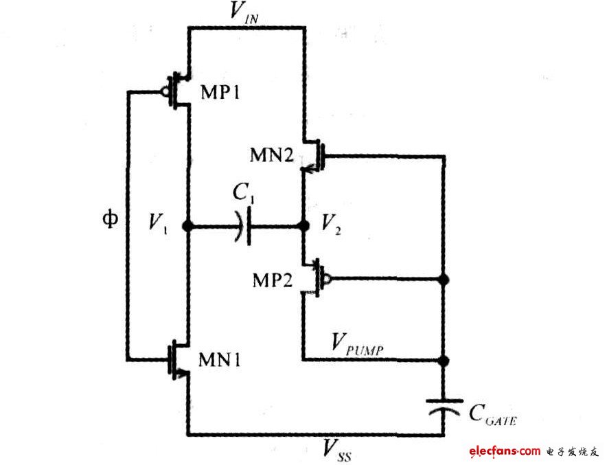
Figure 2 Schematic diagram of the bootstrap charge pump
The bootstrap charge pump does not need to provide gate drive voltages for MN2 and MP2. The control is simple, but the output voltage has a threshold loss. Figure 3 is a circuit diagram of the improved charge pump, with 1 and 2 being complementary non-overlapping clocks. A secondary charge pump consisting of MN2, MN5, MP3, MP2 and capacitor C2 provides gate voltage for MN4 and MP4 to ensure complete turn-off and turn-on. When 1 is low level, MP1 is turned on and the potential is increased. At this time, the potential of V3 is zero, MP4 is turned on, the charge on V2 is transferred to the gate capacitance CGATE, and the potential of VPUMP is raised. When 1 is high level, MP2 is turned on, charging C2, V4 potential rises to the power supply potential, V3 potential rises, MP3 turns on, and VPUMP potential continues to rise. MN3 is equivalent to a diode and acts as a one-way conductor.
After the VPUMP voltage rises to VIN+VT, MN3 isolates the path from V3 to the power supply, ensuring that the charge of V3 is fully charged by the MP3 into the gate capacitance. Thus, C1 and C2 charge the gate capacitance to each other, and after several clock cycles, the charge pump output voltage is close to twice the supply voltage.
During the increase of the charge pump output voltage, the load current provided by the power tube gradually rises to avoid inrush current on the capacitive load.
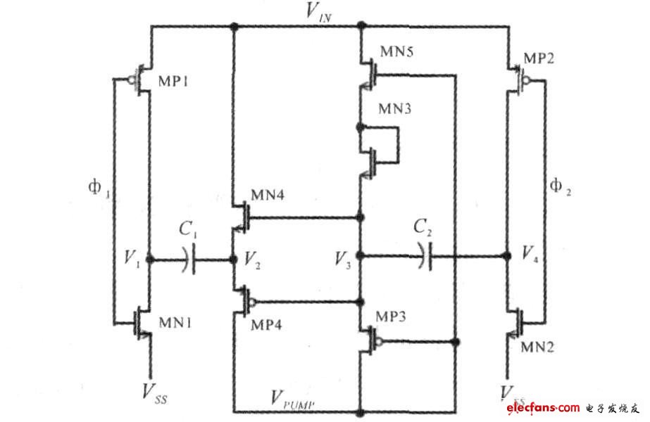
Figure 3 Improved charge pump
Wuxi Juxingyao Trading Co., Ltd , https://www.juxingyao.com