Design scheme of charge pump circuit for white LED driving
0 Preface
The boost type circuits currently used for white light driving mainly include an inductive DC-DC circuit and a charge pump circuit. The inductive DC-DC circuit has problems such as EMI, and the charge pump circuit has a simple structure and a small EMI, and has been widely used.
There are two main types of white light LED driven charge pumps: voltage mode and current mode. Relative to the voltage mode, which may cause the brightness mismatch of each LED, the current mode outputs a constant current separately, so that the brightness can be well matched, and the peripheral balancing resistor is not needed, which greatly saves space.
The design of the current-type charge pump circuit for white LED driving proposed in this paper. The design adopts 1.5 times voltage boosting, which improves the efficiency compared with the traditional 2x voltage boost mode, and adopts digital dimming mode to provide 32 gray scale output to meet the requirements of different occasions. The system structure is shown in Figure 1. Mainly can be divided into the following parts: bandgap reference circuit, soft start circuit, oscillator, 1.5 times charge pump, digital dimming module. When the EN/SET terminal inputs a high level, the chip starts, Vin is boosted by 1.5 times the charge pump to stabilize the output voltage at 5 V. If the EN/SET terminal inputs a series of pulses and then sets a high level, the digital dimming The module can record the number of pulses and then convert them into different output currents to achieve the dimming function.

1 1.5 times charge pump principle
1.1 Basic principles
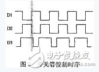
The principle of 1.5 times voltage charge pump is shown in Figure 2. The basic control idea is as follows: OSC controls the conduction and shutdown of S1~S7 through the drive circuit. The timing is as follows: at the first moment, S1, S4, and S6 are turned on, Vin charges capacitor C1, C2 is shorted, VC1=V1, VC2=0; at the second moment, S1, S4, and S6 are turned off, and S2, S3, and S5 are turned on. , S7, C1 charge C2, make VC1=VC2=1/2 V1, and finally add V1 to charge C3, and then cycle again, VCUT is divided by resistor, compare with the reference voltage, control the on-resistance of the upper MOS transistor, change The RC charging constant of the charging circuit finally stabilizes the output at 5 V. Figure 3 shows the timing diagram of the control pulse, where D1 is the driving signal of S1, low effective; D2 is the driving signal of S4, S6, high effective; D3 is S2 The drive signals of S3, S5, and S7 are low effective. In order to prevent clock feedthrough, a non-overlapping clock circuit is included in the driver circuit.

1.2 Actual circuit design
The entire switch network consists of five PMOS transistors S1, S2, S3, S5, S7 and two NMOS transistors S4, S6, as shown in Figure 4. Taking the P pipe S1 and the N pipe S4 as an example, the width to length ratio of the switch pipe is calculated. According to the requirements of the layout design rules, the width/length ratio W/L of a single tube can be set to 2.8 μm/0.6 μm. Suppose the width to length ratio of S1 is x (W/L), and the width to length ratio of S4 is y (W/ L). This design uses CSMC 0.6 μm process, according to process and design requirements, V1=3.3 V, unCOX=50μA/V2 VTHN=0.7 V,|VTHP|=1 V, 2up=un, because

The width to length ratio of other tubes can also be obtained in the same way. Since the current flowing through the switch tube is relatively large, the width-to-length ratio of the switch tube is large, and the transistor is generally connected in parallel, and is usually implemented as a waffle structure on the layout.
If the substrate of the switch is not connected to the source, a substrate bias effect is generated, causing a threshold loss in the switch, causing the charge pump voltage to fail to rise to a set value. As shown in Figure 4, the source and drain terminals of the switches S1, S3, S4, S5, and S6 can be easily judged. The voltages at both ends of S2 and S7 are undetermined, so if the processing is not properly performed, the substrate bias will be caused. Effect, this design uses a way to solve this problem better. V1 and Vout are compared by a comparator. If Vout "V1", the substrate of S2 and S7 is terminated with Vout, if Vout


Heavy Duty Connectors (HDC) provide extensive industrial inserts,
alternate or direct-current connectors for heavy-duty industrial applications; multi-pole connectors for use in electronic machinery, robots, electric panels, control equipment, power and control- or signal-circuit connectivity; enclosures for standard, harsh and EMC environments; plastic and metal cable glands. All products are designed with top-quality materials.
The principal HDC parts are comprised of die-cast aluminum alloy with either a polyester powder (nickel-plated for EMC versions) finish or a self-extinguishing thermoplastic. Coupling stability and accidental opening protection is achieved by two locking systems (mono-block levers in galvanized or stainless steel or springs and pegs in stainless steel). Sealing of dust, water and aggressive agents is assured with internal protective gaskets.
Heavy duty connector
Wonke Electric CO.,Ltd. , https://www.wkdq-electric.com