What are FPGAs, ASICs, and how to design a power supply system for them?
FPGA (Field-Programmable Gate Array), which is a field-programmable gate array, is a product further developed on the basis of programmable devices such as PAL, GAL, and CPLD. It emerged as a semi-custom circuit in the field of application specific integrated circuits (ASIC), which not only solves the shortcomings of the custom circuit, but also overcomes the shortcomings of the limited number of original programmable device gates.
The FPGA adopts the concept of Logic Cell Array (LCA), which includes three parts: Configurable Logic Block (CLB), Input Output Block (IOB) and Interconnect (Interconnect). Field Programmable Gate Arrays (FPGAs) are programmable devices that have different structures than traditional logic circuits and gate arrays such as PAL, GAL, and CPLD devices. The FPGA uses a small lookup table (16&TImes; 1RAM) to implement the combinational logic. Each lookup table is connected to the input of a D flip-flop, which in turn drives other logic circuits or drives I/O, thereby forming a combination. The logic function, in turn, implements the basic logic unit modules of the sequential logic functions that are interconnected or connected to the I/O modules using metal wires. The logic of the FPGA is realized by loading programming data into the internal static storage unit. The value stored in the memory unit determines the logic function of the logic unit and the connection mode between modules or modules and I/O, and finally determines The FPGA allows for unlimited programming.
Currently, the ASIC in the integrated circuit industry is considered to be an integrated circuit designed for a specific purpose. Refers to integrated circuits designed and manufactured to meet the needs of specific users and the needs of specific electronic systems. ASIC is characterized by the needs of specific users. ASICs have the advantages of smaller size, lower power consumption, higher reliability, improved performance, enhanced confidentiality, and lower cost compared with general-purpose integrated circuits in mass production.
ASIC's design methods and methods have evolved over the decades, from the initial full manual design to the now advanced process that can be fully automated. This is also the result of the development of science and technology, especially electronic information technology, in recent decades. From the process of design evolution, the design approach has gone through manual design, computer-aided design (ICCAD), electronic design automation EDA, electronic system design automation ESDA and user field programmable controller stage. Integrated circuits are fabricated on prototype wafers that are only a few hundred microns thick, and each wafer can hold hundreds or even thousands of dies. The complexity of transistor and wiring in an integrated circuit can be made up of many layers. The most complicated process today consists of six layers of diffusion or ion implantation layers inside the silicon wafer and six layers of wiring on the surface of the silicon wafer. composition. As far as design methods are concerned, the methods of designing integrated circuits can be divided into three methods: full customization, semi-customization and programmable IC design.
There are only a handful of power management related design challenges on FPGA, GPU or ASIC-controlled system boards, but due to the need for repeated debugging, such challenges can seriously lag the system's launch time. However, if a specific design or similar design has been verified by the power supply vendor and the FPGA, GPU, and ASIC manufacturers, many power and DC/DC regulation issues can be prevented. The burden of analyzing and solving problems often falls on the shoulders of system designers. The complex digital portion of the configuration design has taken up most of the energy of these designers. So dealing with the analog and power sections of the design is a major challenge, as power is not a simple task as many designers have expected.
Comprehensive power management is challenging from the startAll design tasks are challenging at first, such as designing a power management solution for a complex system that includes transceivers, memory modules, sensors, line connectors, and mesh PCB traces and multilayer PCB planes. However, the confusing use of DC/DC regulators, capacitors, inductors, heat sinks, and other thermal measures, as well as component layouts to address power management designs, can lead to subsequent design issues. If the system designer hastily decided to choose a poor solution, then there may be situations where debugging work can't go on.
Where to start power management designWith a systematic and well-considered design approach, you can start any power management circuit design with great confidence. In other words, before the PCB assembly, if the analysis is accurate and solves the power management-related design challenges, the power management circuit design can be simplified. In addition, the power management guidelines are circuited and tested to meet the requirements of FPGAs, ASICs, GPUs, and microprocessors, as well as systems that use these and other digital components. Designing power management circuits with proven power management solutions will ensure that the project is confident from the start. This is the key to getting the design into the production phase quickly from the prototype stage, as this saves power commissioning time.
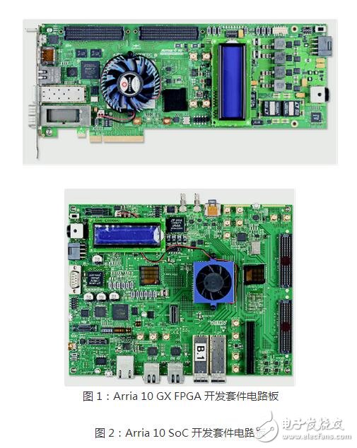
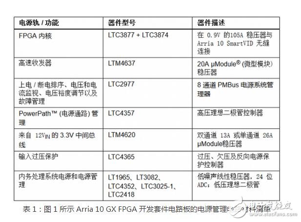
A good example: powering Arria 10 FPGAs and Arria 10 SoCsSystem developers can use FPGA development tools to evaluate FPGAs without having to design a complete system. Figure 1 and Figure 2 show Altera's new 20nm Arria 10 FPGA and Arria 10 SoC (System on Chip) development boards. These boards have been tested and validated by Altera Corporation to list the best design practices for layout, signal integrity, and power management.
Power management for the core, system, and I/O. Power management solutions for high-end FPGAs such as Arria 10 should be carefully chosen.
A well-planned power management design reduces PCB size, weight, and complexity while reducing power and cooling costs. This is essential to optimize system performance.
For example, to provide a 0.95V/105A for the 12V DC/DC regulator powered by the core of the Arria 10 GX FPGA in Figure 1, the DC/DC regulator has several features that complement the SoC's power-saving approach:
Arria 10's SmartVID uses a 6-bit parallel VID interface integrated in a DC/DC regulator to control the DC/DC regulator, reducing FPGA power consumption in both static and dynamic conditions.
The DC/DC regulator uses a very low DCR current detection method to improve efficiency by minimizing power dissipation in the inductor. Temperature compensation maintains accuracy or DCR values ​​when the inductor temperature is high.
Table 1 summarizes the power rails and features of the Arria 10 Development Kit board shown in Figure 1. This table lists the Linear Technology devices and describes the features of each device. Visit, click on Arria to learn more about the technical details of the two boards shown here.
What if the design listed in the development kit does not meet your power requirements? In this case, the PC-based LTpowerPlanner® tool can be used to personalize and optimize the system power tree.
Start with the recommendations given in the development kit; then easily reorganize power components, change power ratings, calculate efficiency and power consumption, simulate each power component, select DC/DC regulator device models, and validate custom solutions.
LTpowerPlanner is one of the more versatile LTpowerCAD® design tools used to generate the power tree (Figure 3) that meets the FPGA requirements and system requirements in the Arria 10 development kit.
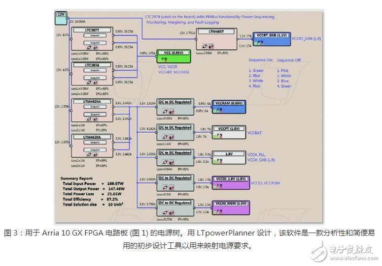
LTC2974 (used on the board) Add PMBus function: power sequencing, monitoring, margining, and fault logging
Loss: Power consumption
Sequence On: Sorting on
Sequence Off: Sorted off
Green: Green
Blue: Blue
White: White
Pink: Pink
DC to DC Regulator: DC to DC Regulator
Summary Report: Summary Report
Total Input Power: Total Input Power
Total Output Power: Total Output Power
Total Power Loss: Total Power Consumption
Total Efficiency: Total Efficiency
Total SoluTIon Size: Overall size of the solution
LTpowerCAD helps users:
· Select a specific Linear Technology DC/DC regulator to match a given power performance specification
· Choose the right power components (eg inductors, resistors and capacitors)
· Optimize efficiency and power consumption
Optimize regulator loop stability, output impedance, and load transient response
· Export the design to LTspice®
in conclusionWe can safely start the power management circuit layout. Tools such as LTPowerCAD and LTPowerPlanner greatly simplify the mapping of load point regulators and the results of individual sections. To illustrate these advantages, this article uses a development kit design guide for Altera Arria 10 FPGAs and SoCs and other Altera FPGAs, including power trees and bill of materials. Information can be obtained by visiting: To learn about the Xilinx FPGA Development Kit, please visit: These development kits are tested and validated by Altera, Xilinx or third-party developers.
Notonthehighstree Notonthehighstree33
Bossgoo(China)Tecgnology.(Bossgoo(China)Tecgnology) , https://www.tlqcjs.com