Specificity of WLCSP package in mechanical properties
WLCSP (Wafer Level Chip Scale Packaging) is designed to reduce chip manufacturing costs and achieve a small number of pins and excellent performance. The wafer level package solution directly solders the die directly to the motherboard. This paper aims to introduce the specificity of this new packaging technology, explore the most common thermal mechanical failure problems, and propose corresponding control schemes and improved methods.
Although wafer-level packaging technology has advantages, there are special thermal mechanical failure problems. Many experimental studies have found that passivation or underlayer rupture, moisture infiltration, and/or die edge delamination are common thermomechanical failure modes for wafer level packaging. In addition, the edge of the die is a particularly sensitive area and we must pay more attention. In fact, the fan-in package die is exposed to the air (without the molding compound surrounding the die), which is easily contaminated or cracked by chemicals. There are many reasons involved, such as unoptimized wafer cutting process and structural defects of the seal ring (the seal ring refers to the metal pattern around the die, which acts as a mechanical and chemical protection). In addition, since the solder balls are very close to the passivation layer, the solder ball process and the line back stack may interact.
In this paper, FEM (Finite Element Method, finite element method) method is used to analyze stress, and the focus is on the fan-in package. We give a typical stress area. To reduce the risk of mechanical failure, we also briefly introduced the specificity of wafer level packaging. After describing the mechanical failure, we also performed a comprehensive analysis of the die and passivation edges. The results of the analysis show that the passivation edge produces the greatest stress, which imposes requirements on the deposition strategy (direct or cone deposition method) and edge location. In addition, the results of the study also show that the residual stress must be reduced and the passivation layer thickness of the BEoL (end of the line) must be increased.
1. Preface and backgroundWafer-level packages are designed to reduce chip manufacturing costs and enable chips with few pin counts and excellent performance. The wafer level package solution directly solders the die directly to the motherboard. Two-layer dielectric, RDL (ReDistribuTIon Layer), UBM (weldable thin layer for solder ball bottom metallization) and solder balls are placed on top of the standard BEoL stack. Therefore, these levels extend the range of conventional wafer processes (multilayer deposited film lithography processes). The solder ball process in wafer level packaging is very similar to flip chip packaging.
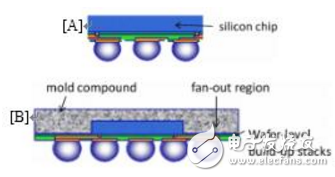
Figure 1: [A] Fan-in package (wafer-level package) and [B] fan-out package (package size depends on the gap between the die edge and the assembly stack)
Wafer-level packages are mainly divided into fan-in and fan-out packages (Figure 1). The fan-in package is a package process that is completed before the wafer is uncut, ie, packaged and then cut. Therefore, the die is packaged to the same size as the die itself (Figure 2 [A]). The fan-out package first rebuilds each die on an artificial molded wafer. The "new" wafer is the substrate on which the RDL wiring layer is processed, and then the final package is completed in accordance with the normal fan-in wafer level packaging process. Process (Figure 2 [B]) [1-2-3-4-5].
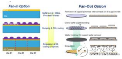
Figure 2: Fan-in and fan-out package processes
It should be noted that in order to improve the reliability of wafer level packaging, there are various solder ball assembly processes, including solder balls on the nitride layer [6], solder balls on the polymer layer [7-8], copper. Column wafer level packaging and more. This article focuses on the method of assembling solder balls with UBM layers on the RDL layer/polymer layer (Figure 3).
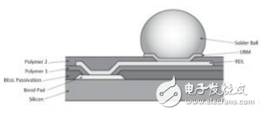
Figure 3: Assembling UBM solder balls with a polymer solution
The next chapter focuses on the unique thermomechanical failures of wafer level packages.
Usb Type C,Usb A To Usb C,Usb A To C Cable,Type-C To Micro-Usb
Dongguan Swan Electronic Technology Co., Ltd , https://www.swanconnector.com