UART Verilog programming
Verilog is a description of complex hardware circuits. Designers always divide complex functions into simple functions. Modules are the basic structure that provides each simple function. Designers can adopt a "top-down" approach to divide complex functional modules into low-level modules. This step is usually done by the system-level chief designer, while the low-level modules are done by the next level of designers. The top-down design facilitates system level tiering and management, and increases efficiency and reduces costs. The "bottom-up" approach is the reverse of the "top-down" approach.
The basic design unit that describes the hardware using Verilog is the module. The construction of complex electronic circuits is mainly achieved through the interconnection of modules. Modules are included in the keyword module, endmodule. The actual circuit components. The modules in Verilog are similar to the functions in C language. They can provide input and output ports, and can call other modules as examples, or can be called by other module instances. The combination logic portion and the process timing portion may be included in the module.
So how is the UART Verilog program designed? Let's take a look at the design of the uart_receiver design and send module uart_transfer. Finally, a detailed introduction to the UART serial communication protocol is provided.
UART Verilog programming:When designing the UART Verilog program, the UART communication protocol we used was: 1 start bit, 8 data bits, no parity bit, and 1 stop bit.
Baud rate: We use 9600 baud rate, but we generate a 9600*16 times baud rate on the FPGA crossover circuit, that is, 16 pulses of the FPGA receive one PC end data. In order to be valid when the RXD data start bit signal is sampled, 0-7-15 starts counting, where 7 is the midpoint of the data and the most stable time. Therefore, sampling data at this time can achieve the most stable effect.
Receiver module uart_receiver design
1) Synchronization of asynchronous data
Since the data on the PC and FPGA side are not synchronized, in order to ensure data synchronization, the external input signal needs to be synchronized. A simple D flip-flop sequential circuit is used.
2) Design of data receiving state machine
State machine allocation table:
R_IDLE: Initialization wait state
R_START: Received start bit 0 (also judged whether it is data jitter)
R_SAMPLE: Receive data
R_STOP: Wait for the stop bit to end and return to the initialization state
3) Design procedure steps:
Two-stage state machine
The first paragraph: using combinational logic to determine the conditions for state transition
(1) The start bit is detected in the initialization state to implement the state transition. R_IDLE
(2) Determine whether the start bit is jittery. At the midpoint detection signal, when the count end (SMP_TOP) data is still valid, it indicates the start of the start bit. R_START
(3) Receive 8-bit data, using point sampling in the data. R_SAMPLE
(4) Waiting for the UART end bit to complete the reception of one frame of data. R_STOP
The second paragraph: synchronous reception using synchronous timing circuits
Finally, the data capture enable signal rxd_flag is output as a capture enable signal for subsequent modules.
Send module uart_transfer design
1) Design of data receiving state machine
State machine allocation table:
T_IDLE: Initialize wait state, waiting for the transmit enable signal
T_START: Data transmission, return to the initialization state after the transmission is completed, waiting for the next transmission enable.
2) Design procedure steps:
Two-stage state machine
The first paragraph: using combinational logic to determine the conditions for state transition
(1) A transmission enable signal is detected in an initialization state to implement state transition. T_IDLE
(2) Send 10-bit data, which is sent at the midpoint of counting. Waiting for the next T_START
The second paragraph: synchronously sequential circuit is used to transmit UART data bit by bit. 10 data needs to be sent in accordance with the UART communication protocol.
Finally, the data transmission completion signal txd_flag is output as an enable signal of the subsequent module.
UART serial communication protocolThe UART uses asynchronous, serial communication.
Serial communication refers to the sequential transmission of data bit by bit using a transmission line. The utility model has the advantages that the communication line is simple, the communication can be realized by using a simple cable, the cost is reduced, and the application is suitable for long-distance communication, but the transmission speed is slow.
Asynchronous communication uses one character as the transmission unit. The time interval between two characters in communication is not fixed, but the time interval between two adjacent bits in the same character is fixed.
The data transfer rate is expressed in baud rate, which is the number of binary bits transmitted per second. For example, if the data transfer rate is 120 characters/second and each character is 10 bits (1 start bit, 7 data bits, 1 check bit, 1 end bit), the baud rate of the transfer is 10 & TImes. ;120=1200 characters/second=1200 baud.
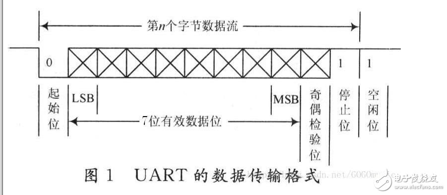
The data communication format is as follows:

The meaning of each of them is as follows:
Start bit: A logic "0" signal is sent first to indicate the beginning of the transmitted character.
Data bits: can be 5~8-bit logic "0" or "1". Such as ASCII code (7 bits), extended BCD code (8 bits).
Check Digit: When the data bit is added to this bit, the number of bits of "1" should be even (even parity) or odd (odd parity).
Stop bit: It is the end of a character data. It can be a high level of 1 bit, 1.5 bits, or 2 bits.
Idle bit: In the logic "1" state, there is no data transmission on the current line.
Asynchronous communication is transmitted by characters. After receiving the start signal, the receiving device can receive correctly by keeping the synchronization with the transmitting device within one character transmission time.
Pos System, Cash Register Terminal,Free Pos Software,Point Of Sale Terminal
Guangzhou Winson Information Technology Co., Ltd. , https://www.barcodescanner-2d.com