Detailed steps and methods for patch antennas to solve diversity and multi-frequency problems
Handheld and portable wireless products, such as smartphones and wearable electronics, rely on microchips, patches, and wire antennas that can be placed into devices. Although these small devices solve the problem of carrying multi-band antenna arrays in small-sized systems, they also introduce problems related to radiation efficiency degradation, impedance matching, and interaction with nearby objects and human bodies.
To solve these problems, designers began to adopt new design and circuit methods, so that these antennas not only become a separate component, but become part of the dynamic antenna subsystem that can solve many of the above design challenges. This design shift requires a lot of simulation and analysis, and the ever-improving field solver software can meet this need.
There are many reasons for the transition from traditional external whip or short antennas to chip and patch antennas. The first and foremost is the aesthetics and fragility of external antennas. From a performance standpoint, devices such as smartphones often require multiple antennas in a given frequency band to provide antenna diversity, which in turn improves performance. In addition, multi-band devices (especially those that are compatible with the emerging 5G standard) require separate, stand-alone antennas in each frequency band they must support. Despite these many reasons, chips and patch antennas have their own short boards.
The chip antenna uses a multilayer ceramic structure to form a component that resonates at the target frequency (Figure 1). Like all other surface mount components, they are small enough to fit easily on a PC board.
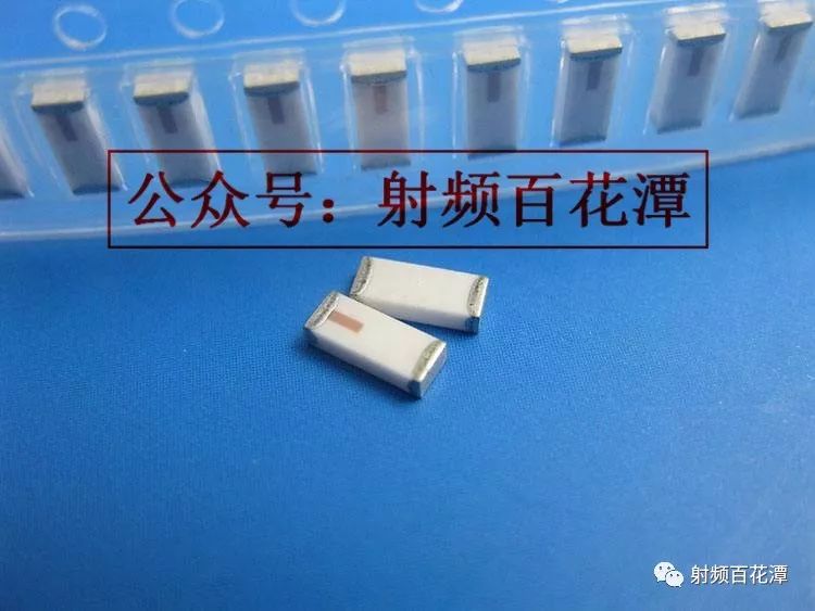
Figure 1: Ceramic chip antennas that are small, low-cost, and easy to apply, many portable wireless devices will not be implemented. The figure shows the Johanson Technology 2450AT18B100E, located in the middle of the widely used 2.4 to 2.5 GHz band. (Source: Johanson Technology)
We use two examples to illustrate their characteristics. The Johanson Technology 2450AT18B100E is a 1.6 x 3.2 mm chip antenna for the 2.4 to 2.5 GHz band, although it is small enough to provide a near-omnidirectional radiation pattern without regard to direction (Figure 2). Antennas like this have been widely used in portable and handheld wireless devices. Although the chip antenna itself is simple, the designer must match the associated driver circuit to its 50 Ω standard impedance. This can be a major challenge when using multiple chip antennas in a diversity architecture.
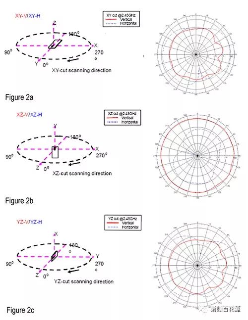
Figure 2: Johanson describes the radiation pattern of the chip antenna on all three axes (top to bottom: a) XY, b) XZ and c) YZ); note that this mode is nearly identical on all three axes. Omnidirectional. (Source: Johanson Technology)
Another chip antenna is the Taiyo Yuden AF216M245001-T, which is used to simulate a single-pole helical antenna that is also suitable for the 2.4 to 2.5 GHz band. The antenna measures 2.5 x 1.6 mm and is also nearly omnidirectional and maintains a VSWR of less than 2:1 in the 2.45 GHz to 2.7 GHz band (Figure 3).
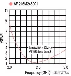
Figure 3: Taiyo Yuden's AF216M245001-T chip antenna maintains a 2:1 VSWR over its main operating bandwidth of 2.45 GHz to 2.7 GHz. (Source: Taiyo Yuden)
Due to their low cost, small size, and ease of use, chip antennas appear to be the optimal solution for many wireless needs. Although this is true in many cases, in reality, like all components, the chip antenna has its own short board. In this case, their typical efficiency is relatively low, only 40% to 50%, and is susceptible to surrounding fixed and changing conditions, including PC board layout, nearby components and users.
An alternative to chip antennas is the patch antenna (Figure 4). Although it is larger than the chip design, it is quite flat, so it can often be placed along the inside of the product casing, away from components and other sources of radiation pattern distortion.
Patch antennas (such as Pulse Electronics' W6112B0100) support 2 x 2 multiple input, multiple output (MIMO) LTE applications including smart meters, remote monitoring and IoT designs. Although the antenna is larger than the chip antenna (approximately 8.8 inches long by 0.8 inches high), it can be as efficient as 55% to 75% depending on the specific frequency band supported (Figure 5).
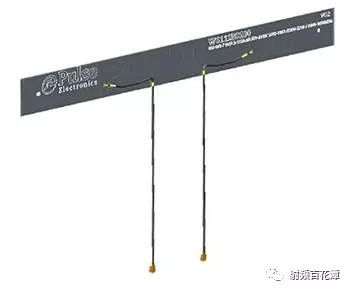
Figure 4: The patch antenna (such as Pulse Electronics' multi-band W6112B0100) is not mounted on the PC board, but is connected to the inside of the product housing, away from the board and circuitry. (Source: Pulse Electronics)
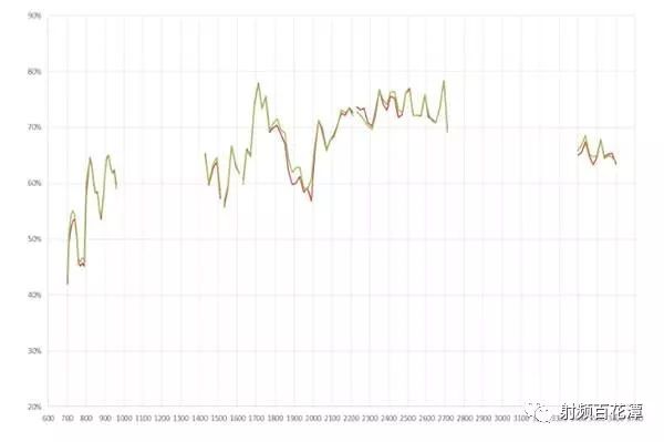
Figure 5: The W6112B0100 for 2 x 2 MIMO 4G/LTE is designed to be 698 MHz to 960 MHz, 1.428 GHz to 1.51 GHz, 1.559 GHz to 1.61 GHz, 1.695 GHz to 2.2 GHz, 2.3 GHz to 2.7 GHz, and 3.4 GHz to It operates in multiple frequency bands such as 3.6 GHz and maintains high efficiency. (Source: Pulse Electronics)
A third type of antenna selection is the PC board trace method, which uses one or more etch layers of the PC board to create the antenna. This solution has no direct BOM cost and is extremely flexible because it can be used to create custom or unique antennas that are not possible with discrete components. A single track antenna can cover multiple frequency bands, including filtering, and support multi-polarization.
But there is no “free lunch†in the world, because the printed circuit antenna often needs a lot of PC board space, and its performance will be greatly affected by the nearby layout, component placement and component types. There is a significant gap between the theoretical line antenna and its actual installation that may be difficult to overcome.
When the system contains multiple antennas and the topology requires switching between antennas, this problem arises – how to implement the handover. Electromechanical switches are effective and have excellent electrical specifications, but this is obviously impractical for small or portable devices and devices that require fast switching. Instead, use an electronic switch, usually a PIN-based diode-based switch (see "How and why a PIN diode is used for a RF switch") or a solid-state switch (see "Semiconductor RF Switch: Small, But High-Performance Circuit Components"). Although PIN diode properties are sometimes required, solid state switches are easier to use and introduce into circuit design than PIN diode based switches.
For example, Peregrine Semiconductor's PE42422MLAA-Z is a basic SPDT RF switch that does not contain any moving parts and is suitable for operation in the 5 MHz to 6 GHz band. When introduced into circuit design, there are fewer design challenges (Figure 6). This 50 Ω component is housed in a tiny 12-lead 2 x 2 mm QFN package that combines on-board CMOS control logic with a low-voltage CMOS-compatible control interface, eliminating the need for external components. It usually completes channel switching in 2 milliseconds.
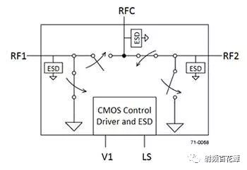
Figure 6: When there are multiple antennas, it is often necessary to switch the RF signal path between the antennas. Pure electronic RF SPDT switches (such as Peregrine Semiconductor's PE42422MLAA-Z) provide a method that can be achieved with simple installation and control, and with a switching time of only 2 milliseconds in the 5 MHz to 6 GHz band. (Source: Peregrine Semiconductor)
The insertion loss ranges from 0.23 dB (100 MHz) to 0.9 dB (6 GHz) with a third-order intercept point (IIP3) of 75 dBm (minimum) over the entire range. This type of switch makes it easy to bidirectionally route RF signals between the universal port and two independent ports with isolation from 68 dB (at lower frequencies) to 17 dB (at higher frequencies). The insertion loss is 0.23 to 1.25 dB, again depending on the frequency.
Using advanced technology to solve real-world problems
The performance of any antenna is affected by its surrounding environment, including nearby components, shielding and packaging. The effects of these elements can be modeled and considered in the final design, but this often requires multiple interactions to achieve a balance of demand conflicts (see "Understanding Antenna Specifications and Operation, Part 1" and "Understanding Antennas" Specifications and operation, Part 2".
But for compact portable and handheld devices, the problem is much more complicated because the surrounding environment of the antenna is constantly changing. The user may hold the product in different directions or near different parts of the body (wrist, head or torso) or place the product near other objects. Therefore, the antenna is in a suboptimal environment where the effective impedance and resonant frequency of the antenna change and performance is degraded.
When the resonant frequency of the antenna shifts, the impedance presented to the rest of the radio front end also deviates from the initial value, causing an impedance mismatch. Impedance mismatch produces three effects. More energy is reflected back from the antenna terminals rather than through these terminals; the output power from the power amplifier (PA) drops due to load pull; and the radiation efficiency of the antenna is reduced due to capacitive loading.
In the past few decades, the situation faced by antennas has led to a decline in the RF link budget, which has affected the performance of the product. This performance degradation has not caught the attention of users due to increased network and system level performance. More cellular base stations, the use of cellular base station antenna beamforming, and improved error correction techniques have largely compensated for this. As system-level requirements and user needs continue to increase, especially for the emerging 5G standards, such compensation may have been “out of the boxâ€.
There are three loss modes associated with this situation: absorption loss, impedance mismatch loss, and antenna radiation efficiency loss. Absorption losses can be as high as 8 to 10 dB, and so far we have nothing to do. The impedance mismatch loss is approximately 1 to 2 dB, while the antenna radiation efficiency loss is approximately 2 to 3 dB. There are two ways to compensate for impedance mismatch and radiation efficiency losses: changing the matching circuit of the antenna and changing the resonance of the antenna.
Wireless device vendors have solved this problem in their latest generation of devices. Dynamic tuning compensates for head and hand effects that cause the antenna's resonant frequency to shift. This is achieved by using a closed-loop tuning period to reduce the mismatch between the antenna and the power amplifier (PA) to optimize power transfer (Figure 7).
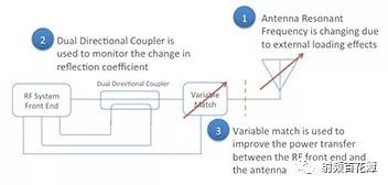
Figure 7: Closed-loop tuning is used to dynamically modify the impedance matching network to achieve optimal performance and reduce losses. (Source: Antennasonline.com)
In closed-loop tuning, the inevitable reflection coefficient changes will be detected in real time. The method is to simultaneously monitor the magnitude and phase of the forward power and reflected power at the antenna terminals through a directional coupler (see "Micro-Directional Couplers Meet the Needs of Compact RF Applications"). The system then synthesizes a complex conjugate for adjusting the matching network at the antenna feed point to enhance RF power transfer between the front end and the antenna. This can reduce losses by as much as 1 to 3 dB.
Although this closed-loop tuning method is useful, there are several disadvantages. Measure the amplitude and phase of the reflection coefficient and then determine the conjugate match, which requires a lot of calculation cycles and time, or a lookup table is needed. Query tables are faster, but with lower precision. To implement complex matching, complex matching circuits are required. The performance gain achieved with this method is typically 1 to 3 dB.
An alternative to closed loop tuning is hole tuning, which is often used in conjunction with impedance matching. In this case, the antenna size (tuned state) will be electrically changed to restore its resonance to the maximum power transfer point instead of adjusting the matching network to accommodate antenna impedance variations (Figure 8). This requires a large number of small pitch tuning states.
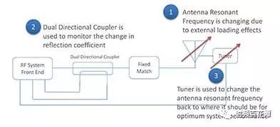
Figure 8. The hole-tuned antenna dynamically adjusts the resonant length of the antenna to minimize losses. (Source: Antennasonline.com)
In this case, as with closed loop tuning, the reflection coefficient will be measured at the feed terminals of the antenna. This measurement is then performed using one of these methods to determine the best new tuning state. Three of these methods are scalar methods that use a simple directional coupler to monitor the amplitude of the reflected power at the antenna terminals and then apply different calculation methods (called square fitting, threshold adjustment, or pit detection).
The fourth method is based on vectors and uses the magnitude and phase of the reflection coefficients to determine the S-parameter matrix solution of the antenna structure, and then determines the tuner settings needed to recover the resonant frequency of the antenna. A loss of 2 to 4 dB is typically reduced. Used in conjunction with impedance matching, the overall improvement range is 3 to 7 dB.
Modeling and simulation that is critical to design success
For external antennas such as standard whip designs, there is little or no performance modeling in the early stages of the design cycle. But for chip, PC board printed line antennas, antenna simulation and its implementation are critical for patch antennas that are very close to low noise amplifiers or power amplifiers. It's impossible to find the right configuration just by building, testing, modifying, repeating, and iterating. Not only must the antenna be modeled, but the entire surrounding environment (PC board, components, enclosure, and even the user's hand or head position) must be modeled and analyzed.
Fortunately, there are many advanced electromagnetic field solver application packages that can solve simulation problems. Supporting them is a powerful PC or cloud-based computing platform that can run the massive calculations required to perform analysis by these field solvers. These field solvers can also analyze the effects of design tolerances by minimum/maximum tests or Monte Carlo runs across multiple variables. They can show that even a fraction of a millimeter of change at GHz can have a significant impact, performing a “what if†analysis to investigate the effects of possible design changes, and highlighting design deficiencies or unexpected features.
to sum upAlthough the function of the antenna is simple, it is a complex electromagnetic sensor that converts electrical power in the circuit into an electromagnetic field and performs reverse conversion. Conventional single element antennas (such as dipole and whip antennas) have now been enhanced to use one or more antennas of multilayer ceramics, flat patch structures, and even the PC board of the product itself.
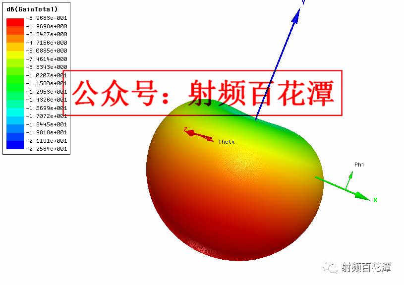
Combining these antennas into a compact (usually portable) product requires careful analysis of the entire system and package, verifying that the idealized performance of the antenna is not greatly affected and can achieve design goals. This can be done using field solver software, which provides powerful support for detailed modeling and correlation calculations of electromagnetic fields and antenna performance in actual installations.
72V Battery Pack ,Lithium Ion Battery Pack,Lithium Battery Pack,Battery Power Pack
Zhejiang Casnovo Materials Co., Ltd. , https://www.casnovonewenergy.com