Use of a sample-and-hold amplifier (THA) in the signal chain to help exceed the ADC sampling bandwidth
The use of a sample-and-hold amplifier (THA) in the signal chain can radically extend the bandwidth beyond the ADC sampling bandwidth to meet the needs of demanding, high-bandwidth applications. This article will demonstrate that adding a THA to the latest converters developed for the RF market will enable bandwidths in excess of 10 GHz. Ps. Broadband as defined herein refers to the use of signal bandwidths greater than a few hundred MHz, with frequencies ranging from DC to 5 GHz to 10 GHz.
Lay the foundation
For radar, instrumentation, and communications applications, high GSPS converters are used extensively because they provide a wider spectrum to extend the system's frequency range. However, the wider spectrum poses additional challenges to the ADC's own internal sample-and-hold, as it is typically not optimized for ultra-wideband operation, and the ADC typically has limited bandwidth, with high-frequency linearity in these higher analog bandwidth regions. /SFDR will drop.
Therefore, using a separate THA in front of the ADC to extend the analog bandwidth is an ideal solution to sample very high frequency analog/RF input signals at a precise time. This process achieves signal sampling through a low-jitter sampler and reduces the dynamic linearity requirements of the ADC over a wider bandwidth because the sample rate remains constant during RF analog-to-digital conversion.
The benefits of this approach are clear: the analog input bandwidth is fundamentally extended, the high-frequency linearity is significantly improved, and the high-frequency SNR of the THA-ADC component is improved compared to the performance of the individual RF ADC.
THA features and overview
ADI's THA Series delivers precision signal sampling over the 18 GHz bandwidth with 9 to 10 linearity, 1.05 mV noise, and <70 fs of random aperture jitter over the DC to over 10 GHz input frequency range. The device operates at 4 GSPS with minimal dynamic range loss, including HMC661 and HMC1061. These track-and-hold amplifiers can be used to extend the bandwidth and/or high frequency linearity of high speed analog to digital conversion and signal acquisition systems.
Taking a single-stage THA HMC661 as an example, the resulting output consists of two segments. In the sample mode interval of the output waveform (positive differential clock voltage), the device becomes a unity-gain amplifier that replicates the input signal to the output stage under the constraints of the input bandwidth and output amplifier bandwidth. During a positive clock to negative clock transition, the device samples the input signal with a very narrow sampling time aperture and maintains the output at a relatively constant value representative of the sampling instant signal during the negative clock interval. When using the ADC for front-end sampling, it is often preferred to use a single-stage device (ADI's simultaneous Fabry two-stage THA model HMC1061) because most high-speed ADCs already have a THA integrated internally, and their bandwidth is usually much smaller. Therefore, adding a THA before the ADC constitutes a composite two-stage component (or a three-level component, if a two-stage HMC1061 is used), and the THA is in front of the converter. With the same technology and design, the linearity and noise performance of a single-stage device is usually better than that of a two-stage device because the number of stages in a single-stage device is lower. Therefore, single-stage devices are often the best choice for front-end sampling with high-speed ADCs.
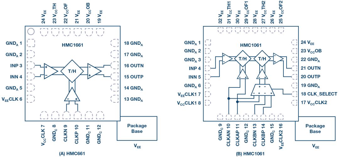
Figure 1. Sample-and-hold topology: (1a) single column, (1b) double column
Delay map THA and ADC
One of the most difficult tasks in developing a sample-and-hold and ADC signal chain is to set the appropriate timing delay between when the THA captures the sample event and when it should be moved to the ADC to resample the event. The process of setting the ideal time difference between two efficient sampling systems is called a delay map.
This process can be tedious on the board because paper analysis may not take into account the corresponding delays caused by the clock trace propagation interval on the PCB, internal device group delay, ADC aperture delay, and splitting the clock into two different segments. Related circuits involved (one clock trace for THA and another clock trace for ADC). One way to set the delay between THA and ADC is to use a variable delay line. These devices can be active or passive in order to properly align the time of the THA sampling process and pass it to the ADC for sampling. This ensures that the ADC samples the stable hold mode portion of the THA output waveform to accurately represent the input signal.
As shown in Figure 2, the HMC856 can be used to initiate this delay. It is a 5-bit QFN package with 90 ps inherent delay, 3 ps or 25 ps, 32-bit high-speed delay. Its disadvantage is to set/traverse each delay setting. To enable the new delay setting, each bit/pin on the HMC856 needs to be pulled to a negative voltage. Therefore, finding the optimal delay setting in 32 combinations by soldering pull-down resistors can be a cumbersome task. To solve this problem, ADI uses serial-controlled SPST switches and off-board microprocessors to help complete delay settings faster. process.
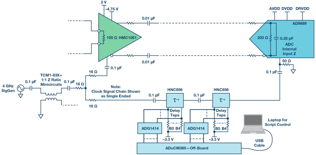
Figure 2. Delay mapping circuit.
To get the best delay setting, apply a signal to the THA and ADC combination, which should be outside the ADC bandwidth. In this example, we select a signal of approximately 10 GHz and apply a level of -6 dBFS (captured on the FFT display). The delay setting is now scanned in binary steps, and the level and frequency of the signal remain constant. The FFT is displayed and captured during the scan, collecting the fundamental power and spurious-free dynamic range (SFDR) values ​​for each delay setting.
As a result, as shown in Figure 3a, the fundamental power, SFDR, and SNR will vary with each setting applied. As shown, when the sampling position is placed in a better place (the THA sends the sample to the ADC), the fundamental power will be at its highest level and the SFDR should be at its best (ie lowest).
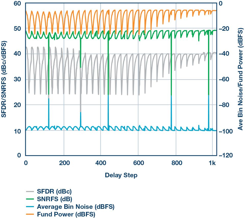
Figure 3a. Mapping results of signal amplitude and SFDR performance for each delay setting.
Figure 3b is an enlarged view of the delayed map scan with a delay setpoint of 671, ie the delay should remain fixed to this window/position. Keep in mind that the delay mapper is only valid for the relevant sampling frequency of the system. If the design requires a different sampling clock, it needs to be rescanned. In this example, the sampling frequency is 4 GHz, which is the highest sampling frequency of the THA device used in the signal chain.
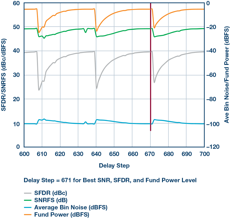
Figure 3b. Mapping results (amplification) of signal amplitude and SFDR performance for each delay setting.
Front-end design for a large amount of raw analog bandwidth
First, if the key goal of the application is to handle 10 GHz bandwidth, we should obviously consider the RF approach. Note that the ADC is still a voltage-type device and does not take power into account. In this case, the word "match" should be used with caution. We found that it is almost impossible to match a converter front end to a 100 MSPS converter at each frequency; RF ADCs with high frequency bandwidths are not much different, but the challenge remains. The term "match" should mean an optimization that produces the best results in the front-end design. This is an all-encompassing term in which input impedance, ac performance (SNR/SFDR), signal drive strength or input drive, bandwidth, and passband flatness all produce the best results for that particular application.
Ultimately, these parameters together define the matching performance of the system application. When starting a broadband front-end design, layout can be critical, and the number of components should be minimized to reduce losses between two adjacent ICs. Both are important in order to achieve optimal performance. Be careful when connecting the analog input networks together. Trace length and matching are the most important, and the number of vias should be minimized, as shown in Figure 4.
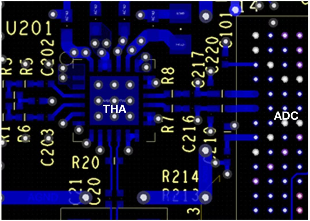
Figure 4. THA and ADC layout.
The signal is connected to the THA input in differential mode (we are also a reference design link that also provides single-ended RF signal input) to form a single front-end network. To minimize the number of vias and total length, we are careful here to keep the vias from passing through these two analog input paths and to help offset any of the traces in the trace connections.
The final design is quite simple, just pay attention to a few points, as shown in Figure 5. The 0.01 μF capacitor used is a broadband type that helps keep the impedance flat over a wide frequency range. A typical finished 0.1 μF capacitor does not provide a flat impedance response and typically causes more ripple in the passband flatness response. The 5 and 10 series resistors at the THA output and the ADC input help reduce peaking of the THA output and minimize distortion caused by residual charge injection into the ADC's internal sampling capacitor network. However, these values ​​need to be carefully chosen, otherwise they will increase signal attenuation and force THA to increase drive strength, or the design may not be able to take advantage of the full range of the ADC.
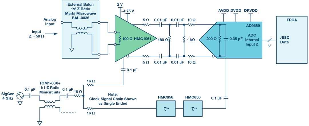
Figure 5. THA and ADC front-end networks and signal chains.
Finally, the differential shunt termination is discussed. This is important when connecting two or more converters together. Typically, light loads (such as a 1 k load at the input) help maintain linearity and pinch the reverberation frequency. The shunt's 120 shunt load also has this effect, but it produces more actual load, in this case 50, which is the load that THA wants to see and optimize.
Look at the results now! Looking at the signal-to-noise ratio or SNR in Figure 6, it can be seen that an 8-bit ENOB (effective number of bits) can be achieved over the 15 GHz range. This is quite good, think about the $13 million you can pay for a 13 GHz oscilloscope of the same performance. As the frequency moves toward the L, S, C, and X bands, the integrated bandwidth (ie, noise) and jitter limits begin to become significant, so we see performance roll-off.
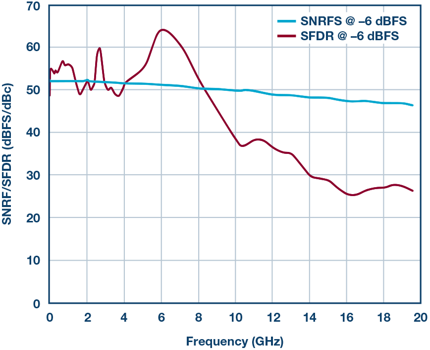
Figure 6. SNRFS/SFDR performance results for –6 dBFS.
It should also be noted that in order to keep the level between THA and ADC constant, the full-scale input of the ADC is internally changed to 1.0 V pp through the SPI register. This helps keep THA in the linear region because its maximum output is 1.0 V pp differential.
Linearity results or SFRD are also shown. Here, the linearity to 8 GHz exceeds 50 dBc, and the linearity to 10 GHz exceeds 40 dBc. To achieve optimum linearity over such a wide frequency range, the design here is optimized with the AD9689 analog input buffer current setting feature (via the SPI Control Register).
Figure 7 shows the passband flatness, demonstrating that adding a THA before the RF ADC can achieve a 10 GHz bandwidth, extending the analog bandwidth of the AD9689.
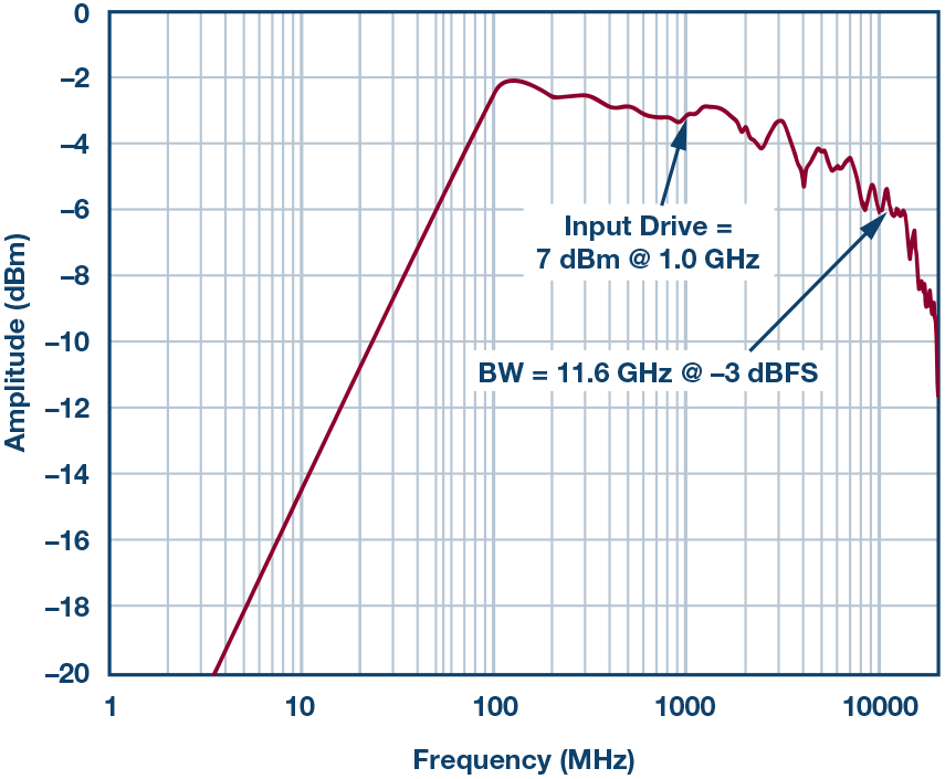
Figure 7. THA and ADC network and signal chain—bandwidth results.
Conclusion
For applications that need to achieve optimal performance on multi-GHz analog bandwidth, THA is almost indispensable, at least for now! The RF ADC is catching up quickly. It is easy to understand that the GSPS converter is theoretically an ease of use when sampling a wider bandwidth to cover multiple target bands, eliminating one or more downmix stages on the front end RF band. However, achieving a higher range of bandwidth can present design challenges and maintenance issues.
When using THA in your system, make sure that the location of the sample points is optimized between THA and ADC. Using the delay map procedure described herein will result in overall optimal performance results. Understanding the program is tedious, but it is very important. Finally, it should be remembered that matching front ends actually means achieving optimal performance for a given set of performance requirements of the application. The LEGO method (simply connecting 50 impedance modules together) may not be the best method when sampling at the X-band frequency.
Lcd Tonch Screen For Iphone 7,Lcd Touch Screen For Iphone 7P,Lcd Display For Iphone 7P,Mobile Lcd For Iphone 7P
Shenzhen Xiangying touch photoelectric co., ltd. , https://www.starstp.com