Read lithography machine: Lithography process flow explain
Semiconductor chip production can be divided into three major areas: IC design, IC manufacturing, and IC packaging and testing. The IC design mainly performs logic design and rule formulation according to the design purpose of the chip, and a mask is prepared according to the design pattern for subsequent photolithography steps. The IC manufacture implements the chip circuit diagram and transfers it from the mask to the silicon chip, and realizes predetermined chip functions, including photolithography, etching, ion implantation, thin film deposition, chemical mechanical polishing and other steps. IC packaging and testing complete the package and performance, functional testing of the chip, is the final process before product delivery.
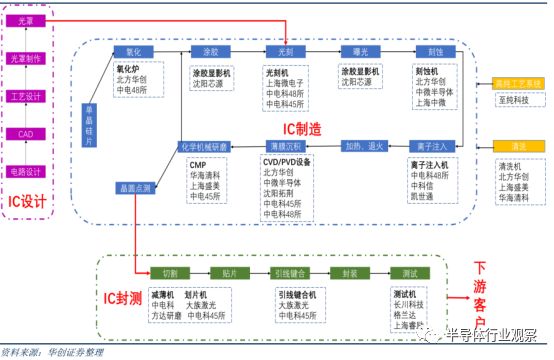
Chip manufacturing core process major equipment panorama
Lithography is the most complex and critical process step in the semiconductor chip production process, which takes a long time and costs high. The difficulty and key point of semiconductor chip production lies in transferring the circuit diagram from the mask to the silicon chip. This process is realized by photolithography. The level of photolithography directly determines the process level and performance level of the chip. The chip requires 20-30 lithography during production, which takes up about 50% of the IC production process and accounts for 1/3 of the chip production cost.
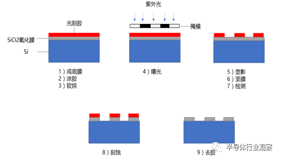
Detailed photolithography process
The principle of photolithography is to cover the silicon surface with a layer of highly photo-sensitive photoresist, and then use light (usually ultraviolet light, deep ultraviolet light, extreme ultraviolet light) to shine through the mask on the surface of the silicon wafer. The irradiated photoresist reacts. After that, the irradiated/non-irradiated photoresist is washed with a specific solvent, and the transfer of the circuit diagram from the mask to the silicon wafer is realized.
After the photolithography is completed, the portion of the silicon wafer not protected by the photoresist is etched, and finally the remaining photoresist is washed away, and the semiconductor device is built on the surface of the silicon wafer.
Photolithography is divided into two basic processes: positive photolithography and negative photolithography. The difference is that the type of photo-resist used by the two is different. Photoresists used in negative lithography will become insoluble after crosslinking due to cross-linking, and will harden, and will not be washed away by the solvent, so that part of the silicon will not be eroded in the subsequent process. The pattern on the photoresist is the inverse of the pattern on the mask.
The process of building a semiconductor device on the surface of a silicon wafer
Positive photolithography, in contrast to negative photolithography, exposes portions of the photoresist that are destroyed and are washed away by the solvent. This portion of the silicon wafer is not etched away by the photoresist, and positive photoresist is applied to the photoresist. The graphic is the same as the graphic on the reticle.
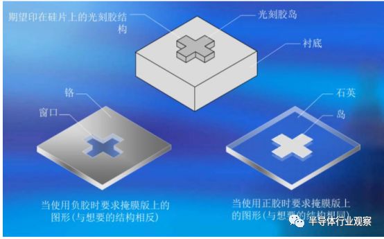
Positive photolithography and negative photolithography
1) Gas-phase film
After cleaning and baking, the silicon wafer is firstly formed into a base film by hexamethyldiamine alkoxide by soaking, spraying or chemical vapor deposition (CVD). The base film separates the surface of the silicon wafer from the water molecules and enhances the photoresist. Binding force. The nature of the base film is as a bonding agent for the silicon wafer and the photoresist and is chemically compatible with these materials.
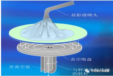
2) Spin coating
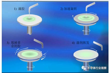
Rotary gluing step
After the bottom film is formed, the photoresist is evenly covered on the surface of the silicon wafer. At this point the silicon wafer is placed on a vacuum chuck, and the bottom of the chuck is connected to a rotating motor. When the silicon is stationary or rotating very slowly, the photoresist is dropped on the silicon wafer. Then accelerate the rotation of the silicon wafer to a certain speed, the photoresist spreads to the surface of the entire wafer by means of centrifugal action, and continues to spin off the excess photoresist to obtain a uniform photoresist film coating layer on the silicon wafer. Until the solvent evaporates, the photoresist film is almost dry and stops.
Coating equipment
3) soft bake
After the photoresist is coated, the silicon wafer needs to be soft-baked to remove the residual solvent in the photoresist and improve the adhesion and uniformity of the photoresist. Photoresists that are not soft-baked tend to be sticky and subject to particle contamination, the adhesion is insufficient, and there is a difference in solubility during development due to too high solvent content, making it difficult to distinguish between exposed and unexposed photoresists.
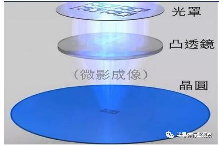
4) Exposure
In the exposure process, after the surface of the silicon wafer is aligned with the quartz mask and focused, ultraviolet radiation is applied to expose the photoresist that is not masked by the mask, and the circuit diagram is transferred from the mask to the silicon wafer.
5) Development
Lithography schematic
A chemical developer is used to dissolve the photoresist-solubilized areas caused by the exposure, allowing the visible pattern to appear on the silicon wafer, and distinguish between areas that need to be etched and areas protected by the photoresist. After the completion of the development, spin off excess developer solution, rinse with high-purity water, and spin dry.
Development process diagram
6) Hard film
After the development of the thermal bake is called hardening film baking, the temperature is higher than the soft bake, the purpose is to evaporate the remaining solvent to harden the photoresist, improve the photoresist on the silicon surface of the adhesion, this step on the lithography The stability of the glue is critical to subsequent etching and other processes.
7) Detection
The results of the silicon wafers were examined, and the qualified silicon wafers were subjected to subsequent etching and other processes. Unqualified silicon wafers entered the initial flow after cleaning.
8) Etching
Etching is the process of selectively removing unwanted materials from the surface of a silicon wafer by chemical or physical methods, and the desired electronic devices can be built on the silicon wafer by etching.
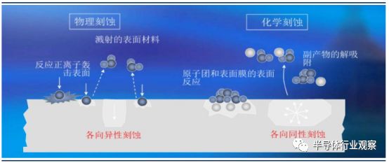
Dry (physical) and wet (chemical) etching schematics
Etching can be divided into dry etching and wet etching. The dry etching exposes the surface of the silicon wafer to an inert gas, and the plasma generated by the gas bombards the window opened by the photoresist and reacts with the silicon wafer to remove the exposed surface material. The etching is performed on the submicron-size etching device. The main method. Wet etching uses liquid chemicals (acids, alkalis, organic solvents, etc.) to chemically remove
In addition to the material on the silicon surface, it is generally used only for larger sizes.
9) Remove glue
After the etching is completed, the photoresist remaining on the surface of the silicon wafer is washed away with a specific solvent.
Lithography machine: The crown jewel of the semiconductor manufacturing industry
The lithography machine can be divided into a lithography machine for producing a chip and a lithography machine for packaging according to different application processes. The package lithography machine has a higher requirement for lithography accuracy and control accuracy than a manufacturing lithography machine. It is much lower and the amount of value is relatively low. This article focuses on lithography machines for chip manufacturing.
The lithography machine is the core device in the lithography process in chip manufacturing. The technical content and value content are extremely high. The lithography machine involves a number of advanced technologies such as system integration, precision optics, precision motion, precision material transfer, and high-precision microenvironmental control. It is the highest-technical device in all semiconductor manufacturing equipment, and therefore has a very high single-unit value. At present, the world’s most advanced ASML EUV lithography machine has a unit price of nearly 100 million euros, which can satisfy the production of a 7-nm process chip.
The working principle of the lithography machine: The lithography machine passes a series of light source energy and shape control methods, transmits the light beam through the mask drawing the circuit diagram, compensates various optical errors through the objective lens, and scales the circuit diagram to map to silicon. On-chip, then developed using chemical methods, resulting in a circuit diagram engraved on the silicon wafer. Different lithography machines have different imaging ratios, 5:1 and 4:1. The internal structure of the lithography machine is shown in Figure 9.
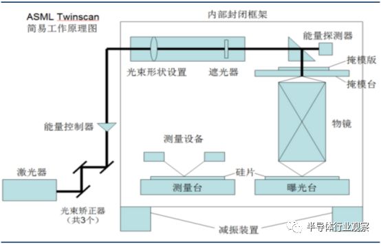
Lithography machine working principle diagram
The internal components of the lithography machine are as follows:
Laser: Light source, one of the core equipment of the lithography machine.
Beam Corrector: Correct the incident direction of the beam and make the beam as parallel as possible.
Energy Controller: Controls the energy that will eventually shine on the silicon wafer. Underexposed or overexposed will seriously affect the imaging quality.
Beam shape setting: Set the beam to round, ring and other shapes, different beam states have different optical characteristics.
Shutter: Blocks the beam from shining on the wafer when exposure is not needed.
Energy detector: Detects whether the final incident energy of the beam meets the exposure requirements and feeds it back to the energy controller for adjustment.
A mask plate: A glass plate engraved with a circuit diagram on the inside, costing hundreds of thousands of dollars.
Masking station: The equipment that carries the mask movement, the motion control precision reaches nano level.
Objective: The objective lens consists of more than 20 lenses. Its main role is to scale down the circuit diagram on the mask, and then it is laser-mapped on a silicon wafer. The objective lens also compensates for various optical errors. The technical difficulty lies in the difficulty of designing the objective lens and the high precision requirements.
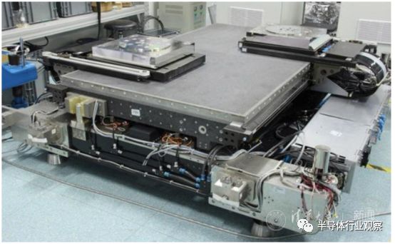
Metering and Exposure Stations: Workstations that carry silicon wafers. General lithography machines need to measure, then expose, only one worktable. ASML's dual-stage lithography machine can achieve one wafer exposure and another silicon. Tablets for measurement and alignment work can effectively improve work efficiency.
Internal closed frame and shock absorber: isolate the work table from the external environment, maintain the level, reduce the external vibration interference, and maintain a stable temperature and pressure.
The development of lithography machines is essentially to meet the production requirements of higher performance and lower cost chips.
Semiconductor chips have different manufacturing processes, that is, different technology nodes. The words 45nm, 28nm, and 10nm that are often seen are descriptions of different processes. How do you understand different processes? What are the differences between different process chips?
This is to be said from the transistor of the most basic unit of the integrated circuit: The transistor is made of semiconductor using its special conductive ability to transmit 0 or 1 digital signal.
The internal structure of the transistor is shown in the figure below. Under the condition that the gate is not energized, the source signal can hardly pass through the non-conducting P-type substrate to the drain region, indicating that the circuit is turned off (digital signal 0) if it is on the gate. When voltage is applied between the region and the substrate, the charge in the substrate will be concentrated under the insulating oxide layer under the action of the opposite attracting, forming a narrow conductive region, making the source region and the drain region conductive, and the current It can pass from the source area to the drain area (signal 1) smoothly. This is the basic operation principle of the transistor. The distance between the two N-wells below the gate, the length of the conductive channel, is defined as the size of the transistor.
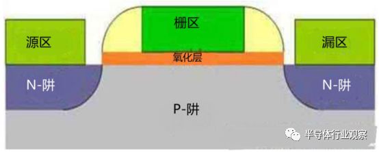
The internal structure of the transistor
In modern transistors, the speed of electrons is limited and generally operates at saturation speed. Therefore, the speed of information transmission is determined by the length of the conducting channel. The shorter the channel, the faster the information is transmitted.
The process of the chip can be approximately understood as the length of the conductive channel of the internal transistor, and the chip with a small process has two advantages:
Processing speed. The small transistor internal transistor has a short conduction channel and a fast signal transmission rate. The chip can process more information per unit time and the clock frequency is higher. The performance per unit area increases and the cost decreases. The smaller transistor size means that the chip can produce more transistors per unit area, chip integration is improved, that is, the function of the chip is increased, and the cost of the unit chip is also reduced. The level of photolithography determines the size of the transistor, so the shrinking of the chip process will inevitably accompany the continuous upgrading and innovation of the photolithography machine products. Essentially, it is the semiconductor industry that is constantly improving the performance and lower cost of the chip. The pursuit promoted the continuous innovation and development of lithography machine equipment.
The lithography machine is the key to the continuation of Moore's Law. Moore's Law states that when the price does not change, the number of components that can be accommodated on the integrated circuit will double every 18-24 months, and the performance will also double. The first 30 years of semiconductor industry development can basically meet Moore's Law, the key is that the lithography machine can continue to achieve a smaller level of resolution. The interval between Moore's Law has been extended to 3-4 years in the past decade. The reason is that the development of the lithography machine is lower than the industry's expectations.
Lithography machine development history: light source improvement + process innovation to promote the replacement of lithography machine
The minimum resolution, productivity, and yield of the lithography machine are all constantly evolving. The minimum resolution of the lithography machine is expressed by R=kλ/NA, where R represents the smallest resolvable size. For lithography, R is the smaller the better; k is the process constant; λ is the light source used by the lithography machine. Wavelength; NA represents the numerical aperture of the objective lens, which is related to the refractive index of the light propagation medium. The greater the refractive index, the greater the NA. The development of the lithography process technology level follows the above formula. In addition, the internal structure and working mode of the lithography machine are also developing, and the production efficiency and yield of the chip are continuously improved.
According to the improvement of the light source used, the lithography machine has experienced the development of the 5th generation product, and each time the light source improvement significantly enhances the minimum process node that the lithography machine can achieve. In addition, the innovation and development of new lithography technologies such as dual-tables and immersive lithography are also continuously improving the level of process technology of the lithography machine, as well as the efficiency and yield of production.
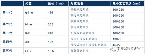
According to the light source used, the lithography machine has experienced the development of five generations of products
The first two generations of lithography machines used 436nm g-line and 365nm i-line produced by mercury lamps as lithography sources, which can meet the production of 0.8-0.35 micron process chips. The earliest lithography machines used contact lithography, ie masks were affixed to a silicon wafer for lithography, which was prone to contamination and had a short mask lifetime. Since then, the proximity lithography machine has improved the contact lithography machine, through the air cushion to create fine gaps between the mask and the silicon wafer. The mask and the silicon wafer are no longer in direct contact with each other. However, the accuracy of the imaging is not high due to the air cushion. .
The third-generation lithography machine uses a 248-nm KrF (niobium fluoride) excimer laser as the light source to raise the minimum process node to the 350-180nm level. In the photolithography process, scanning projection lithography has also been adopted, ie, now lithography. General machine, the light source through the mask, adjusted and compensated by the optical lens, in a scanning manner to achieve exposure on the silicon.
Fourth-generation ArF lithography machine: The most representative lithography machine product. The light source of the fourth-generation lithography machine used a 193-nm ArF (argon fluoride) excimer laser to raise the minimum process to 65 nm in one stroke. The fourth-generation lithography machine is currently the most widely used lithography machine, and is also the most representative lithography machine. Because the lithography machine that can replace ArF to realize the lower process has been unable to develop successfully, the lithography machine manufacturer carries on a large number of technological innovations on the ArF lithography machine, in order to meet the smaller process and higher efficiency production demand.
Innovation 1: Achieve step-by-step scanning projection. In the previous scanning projection lithography machine, the silicon wafer was in a stationary state during photolithography, and the exposure of different areas of the silicon wafer was achieved through the movement of the mask. In 1986, ASML first introduced a stepper scanning photolithography machine, which realized the simultaneous movement of masks and wafers during the photolithography process, and used a reduced projection lens, reducing the ratio to 5:1, effectively improving the mask Using efficiency and exposure accuracy, the chip's process and production efficiency have been raised to a new level.
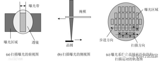
Stepped projection diagram
Innovation 2: Dual-table lithography machine. The silicon wafer must be measured and aligned before entering the photolithography process. In the past, the lithography machine had only one stage. Measurement, alignment, lithography, and other processes were performed on this stage. In 2001 ASML introduced the TWINSCAN system. The dual stage system allows the lithography machine to perform exposure without the need to change the initial speed and acceleration. At the same time, pre-alignment work before the exposure, so that the production efficiency of the lithography machine increased by about 35%.
Although from the results point of view, only one workbench is added, but the technical difficulty is not to be underestimated. The dual workbench system has extremely high requirements for the speed and precision of the exchange. If the exchange speed is slow, then the light will affect the light. Engraving machine work efficiency; If the channel changing accuracy is not enough, it may affect the normal development of subsequent scan lithography and other steps.
Dual table lithography machine prototype
Innovation III: Immersion lithography system. At the 45nm process node, the ArF lithography machine also encountered the problem of insufficient resolution. At this time, the industry has proposed two roadmaps for the development of the next generation lithography machine. One is to develop a 157nmF2 excimer laser with a lower wavelength as a light source, and the other is immersion lithography proposed by Taiwan Semiconductor Manufacturing Co., Ltd. Lin Benjian in 2002. All the previous lithography machines were dry-type machines. Exposure and development were performed in a clean room using air as the medium. Since the NA in the minimum resolution formula is positively related to the refractive index, the minimum resolution will be improved if photolithography with water having a refractive index greater than 1 is used as the medium. This is the principle of the immersion lithography system.
ASML pioneered the introduction of immersion lithography machines to establish its market position. Lin Benjian proposed the concept of immersion lithography, ASML began cooperation with Taiwan Semiconductor Manufacturing Co., Ltd. to develop immersion lithography machine, and in 2007 successfully launched the first immersion lithography machine TWINSCANXT:1900i, the device uses a refractive index of 1.44 deionized water As a medium, the 45nm process technology was realized, and monopolized the market at one go. At that time, the other two major lithography giants Nikon, Canon's main 157nm light source dry lithography machine was abandoned by the market, not only lost a huge manpower and material resources, but also significantly behind the ASML product line, which is also Nikon, Canon by Sheng turn Decline, an important turning point for the ASML family.
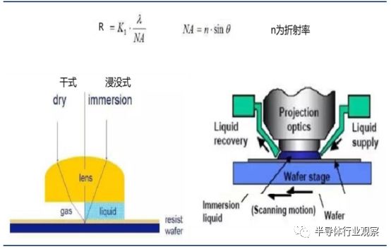
Immersion lithography principle
Through immersion lithography and double lithography processes, the fourth-generation ArF lithography machine can realize the production of chips up to 22nm process. However, under the impetus of Moore's Law, the semiconductor industry's demand for chip processes has been developed to 14nm, 10nm, Even 7nm, ArF lithography machines can no longer meet this demand, and the semiconductor industry hopes to ship to the fifth-generation EUV lithography machine.
The fifth-generation EUV lithography machine came out after a long time. The light sources used by the 1-4 generations of lithography machines are all deep ultraviolet light, and the fifth-generation EUV lithography machines use extreme ultraviolet light with a wavelength of 13.5 nm.
As early as the 1990s, the concept of the EUV lithography machine has been proposed. ASML also started the research and development of the EUV lithography machine in 1999. It was originally planned to introduce the product in 2004. However, it was not until 2010 that ASML developed the first prototype of the EUV. It only delivered downstream customers in 2016, more than ten years later than expected. Samsung, Taiwan Semiconductor Manufacturing Co., and Intel jointly acquired ASML to promote the development of EUV lithography machines.
There are two main reasons for the continuous delay of the EUV lithography machine's time-to-market schedule. First, the required power of the light source can not reach the operating power requirement of 250 watts. Second, the optical precision of the optical lens and mirror system is required. Extremely high, production is extremely difficult. These two major reasons make it difficult for ASML and its partners to support large research and development expenses. In 2012, Samsung's three major customers, Samsung, TSMC, and Intel jointly invested 5.265 billion euros in ASML to support the development of EUV lithography machines. Since then, ASML has acquired Cymer, the world's leading supplier of excimer lasers, and has invested EUR 1 billion in cash to acquire optical system supplier Carl Zeiss to accelerate the development of EUV light sources and optical systems. These two acquisitions have also been successful in the development of EUV lithography. important reason.
The semiconductor industry is now entering a new era.
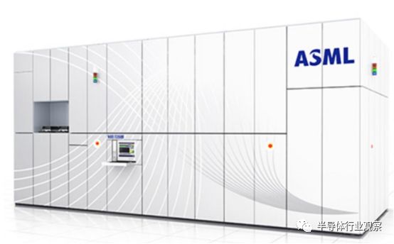
ASMLTWINSCAN NXE: Model 3350B EUV lithography machine
MINI-DP Cable,Mini DP Cable,Mini Displayport Cable,Mini DP 144hz,Mini Displayport Cable
Dongguan Tuojun Electronic Technology Co., Ltd , https://www.fibercablessupplier.com