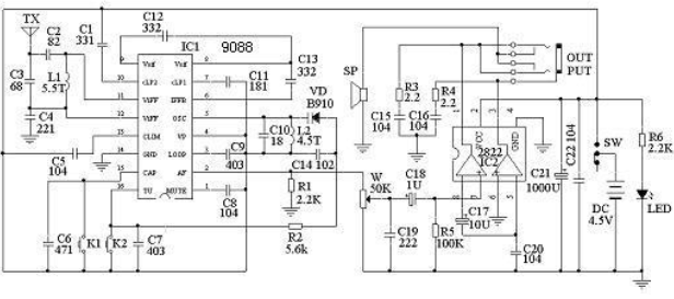
cd9088 circuit principle and debugging method based on CD9088 radio circuit...
The FM signal is introduced by the antenna and enters the mixing circuit from pin 11 of the CD9088 integrated block. Inductance L1, resistor R1, capacitors C1, C2, and C3 form the input loop. The local oscillator frequency of the local oscillator circuit is determined by L2, C4 and varactor D1. . C7 is an audio squelch capacitor, C8 is an intermediate frequency feedback capacitor, C9 is a low-pass filter capacitor, C10 is an intermediate frequency coupling capacitor, pin 15 is the search tuning terminal, pin 16 is the electrical tuning AFC voltage output terminal, and SB1 is the reset button. SB2 is the tuning button. Press the SB2 button and the radio will automatically select stations from the low end of the frequency to the high end of the frequency. When a station is received, it will automatically lock the station to stop searching. If you want to listen to the next radio program, you can press the SB2 button to search for stations in order. When the highest frequency is found, press the SB1 button to return to the lowest frequency, and then select the channel again.
The radio signal received by the antenna input loop is mixed with the local oscillator frequency to produce a 70kHz intermediate frequency signal. After filtering and amplifying by the RC intermediate frequency filter, it is sent to the frequency discrimination stage for processing, and then the audio composite signal is output, after passing through the squelch circuit, the audio composite signal is output from the 2 pin of CD9088, after de-emphasis circuit R3, C15, coupled by C16 It is amplified by the low frequency amplifier circuit composed of VT1 and VT2 to promote the earphone playback. The two inductance coils L3 and L4 are high-frequency chokes. When the earphone lead is used as the antenna, it can reduce the influence of other radio loops on the antenna input loop signal. If a drag line is used as an antenna, disconnect the dotted line. There are advantages and disadvantages to using earphone leads as antennas and towing cables as antennas, which can be determined after testing, or both can be used at the same time. When using the earphone lead as an antenna, the R1 resistance can be omitted.
In the low-amp circuit, the potentiometer is connected to the load loop. It has two advantages: one is that the noise is less than the 2-pin output terminal connected to the CD9088, because the potentiometer itself is connected to the rear stage The noise will not be amplified; second, after the potentiometer is connected to the rear stage, when the volume is turned down, the equivalent resistance of the load will increase, and the working current of the power amplifier stage will be reduced accordingly, so it can reduce battery consumption and extend battery life Service life.
The frequency range of the pocket tuned FM radio is 88-108MHz, and the channel interval is 200KHz. Its main technical indicators: (1) Power supply voltage: 3V; (2) Power consumption current 7~15mA; (3) Sensitivity: 5uV; (4) Signal-to-noise ratio: 50dB; (5) Harmonic distortion (△F=士22.5KHZ): 1%; (6) Audio output power (RL=64Ω): 2~5mW; (7) Audio bandwidth: 125-12000 Hz.
Selection and production of components. The FM ASIC CD9088 can also be selected as the D7088 product of Huayue Microelectronics Co., Ltd. In addition, the SC1088, SL1088, TDA7088 and other types of integrated circuits have exactly the same performance and pins as the CD9088 integrated circuit, and they can also be directly substituted for each other. Capacitors C1~C5, C8~C11 should be small-volume high-frequency ceramic chip capacitors; resistance should be 0.125W metal film resistors; RP1 should be 3386P type sealed metal ceramic miniature single-turn square potentiometers, or general semi-variable Potentiometers and dials are made of plastic materials; D1 varactors use BB910 varactors; SB1 and SB2 button switches use miniature touch button switches; L1, L2 are air-core inductance coils, and L1 uses a 0.43mm diameter High-strength enameled wire is formed by tightly winding 13 turns on a drill shank with a diameter of 2mm. L2 uses the same material and method to tightly wound 10 turns for standby; inductors L3 and L4 use a diameter of 0 on the I-shaped core in the middle. The 27 high-strength enameled wire is wound about 10 times, then glued with polyester tape, and then wrapped with self-adhesive tape for insulation. The earphone adopts an earphone with an impedance of 32Ω, preferably a higher impedance earphone, or two Use the earphones in series to improve the matching of load impedance and increase the sensitivity of the earphones, while reducing the power consumption of the whole machine. When the components are assembled, the pins should be as short as possible to reduce distributed capacitance. CD9088 is a dual-row flat integrated circuit, which is directly soldered on the copper pad of the printed circuit. Before soldering, look for the pins of CD9088 and align with the pin number on the printed circuit. Then solder carefully to prevent tin between the pins. The device is soldered on the component side of the printed circuit board. The two coils of L1 and L2 should be perpendicular to each other during welding to reduce the influence between the mutual circuits. Try not to deform the L1 coil during welding to avoid changing the inductance. SB1 and SB2 can be soldered on the printed circuit board or installed on the shell, and then connected with the lead wire, but the lead wire should be as short as possible. Stereo headphone jack is used to match the stereo headphones currently on the market. After the components are welded, it is best to fix the capacitors of L1, L2 and nearby components with high-frequency paraffin to improve the stability of the receiving frequency. But do not use ordinary candle oil to fix it, so as not to increase the loss and reduce the receiving sensitivity. Debugging can be carried out after all components are installed and checked. When the circuit is not connected to the earphone, the current consumption is about 5mA, and the total power consumption when listening at the maximum volume is about 15mA.
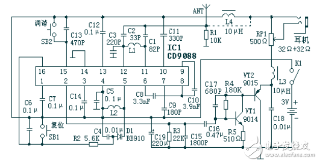
The debugging method is very simple, that is, adjusting the density of the turns of the coil L2 to adjust the range of the radio receiving frequency. If the radio at the high end of the frequency cannot be received, the coil can be pulled apart; if the radio at the low end of the frequency cannot be received, the coil can be clamped a little. Two simple amateur debugging methods are introduced below.
1. Use two new batteries to form a 3V battery pack, use a 1KΩ multi-turn potentiometer and connect it to the 3V battery pack, connect the potentiometer to the negative terminal of the battery pack to the ground wire of the radio, and set the potential The center sliding pin of the device is connected to pin 16 of CD9088, and then the frequency of the radio is adjusted, and the DC debugging voltage output to pin 16 is adjusted to be 0.1V lower than the power supply voltage used by the radio, and then the oscillation coil L2 The spacing is to adjust its inductance so that the radio receives the radio signal at the low end of the frequency about 88MHz, and then adjust the DC debugging voltage to a voltage value that is 1.6V lower than the power supply voltage used by the radio, and it should be able to receive the high end of the frequency about 108MHz Radio signal. If you cannot receive a radio signal of around 108MHZ, you can adjust the frequency coverage by opening some L2 coil spacing. The frequency coverage can be adjusted carefully and repeatedly several times. After the adjustment is complete, remove the battery pack DC debugging power supply, that is, the whole machine debugging is completed. At this time, the receiving frequency of this machine should be in the range of 88~108MHz.
If there is no local FM radio signal close to the low end of the frequency and the high end of the frequency, the approximate DC debugging voltage Vâ–³ of the received FM radio signal frequency can be calculated according to the following method. Then use the Vâ–³ voltage for frequency debugging.
Vâ–³= VH.(f-fL)/(fH-fL)
In the formula: f-receiving frequency; fL-low-end frequency, take 87MHZ; fH-high-end frequency, take 108MHZ;
VH-corresponding debugging voltage of high-end frequency; Vâ–³-DC debugging voltage of a certain frequency (VCC-Vs);
Vs-the DC debugging voltage applied to the ground on pin 16 at a certain frequency.
Example: Seeking to receive the 16-pin DC debugging voltage Vâ–³ of a 102MHZ frequency for an FM radio station.
That is, Vâ–³=VH.(f-fL)/(fH-fL)
= 1.6&TImes;(102-87)/(108-87)
≈1.14(V)
Debug the 16-pin DC debugging voltage Vâ–³ at 1.14V, and then turn a little or close the turn-to-turn spacing of the L2 coil to fine-tune the frequency, so that the FM radio signal with a frequency of 102MHZ will be received; then look for a signal close to the low-end frequency For the FM radio signal, use the same method to obtain the Vâ–³ voltage, and then fine-tune L2 to receive the FM radio station. After several considerations, when receiving the above two FM radio stations separately, watch the two Vâ–³ voltages close to the calculated value. The debugging is complete.
(2) Press and hold the SB1 reset button, toggle the L2 coil spacing, and change its inductance to receive an FM radio signal of about 88MHZ. If you receive an FM signal of about 92MHZ, you can close the L2 coil slightly. If the high-end receiving frequency range is not enough, you can refer to the method (1) and then fine-tune the L2 coil spacing. When adjusting the frequency range, an FM radio with a frequency scale should be used as the receiving frequency reference. Because the machine uses buttons to electrically tune and adjust the radio station, there is no need to make cumbersome frequency scales, so it is easy to make and configure a beautiful radio shell.
The pocket-sized campus electronically tuned FM radio can be used normally after simple debugging. Suitable for experimental production of amateurs.
Not only fashionable, but also protective. Our protective sleeves provide impact protection, shock absorption and a slim design. The Phone Case can give you peace of mind and provide better protection. If you keep your phone clean and scratch-free, you can also increase the resale value of your phone.
Design: The fit design makes your phone slimmer.
Protection: These Mobile Phone Case have been tested to withstand those accidental drops. The inner layer is made of Soft TPU rubber material, and the reinforced corners can absorb impact. High lips recess your screen and camera to provide additional protection. The outer hard shell is impact resistant.
Function: When all ports can be accessed, your phone can be used normally. The Cell Phone Case has molds for volume buttons and power buttons, so it is protected and you can still feel/use them.
If you want to know more about Mobile Phone Case products, please click the product details to view the parameters, models, pictures, prices and other information about Mobile Phone Case.
Whether you are a group or an individual, we will try our best to provide you with accurate and comprehensive information about the Mobile Phone Case!
Matte Phone Case, Marble Phone Case, Protective Case, Iphone Case, Transparent Phone Case, Protective Cover
Shenzhen Jianjiantong Technology Co., Ltd. , https://www.jjtphonesticker.com