Redmi Note3 mobile phone disassembly method picture summary
Redmi Note3 Standard Edition, running memory 2GB, storage memory 16GB.
First take out the phone card tray with a card extractor.
Use an opening pick to insert the gap of the back cover and slowly pry out. After the back cover is pried out, pay attention to that there is a fingerprint unlocking module cable connected to the motherboard.
Use an opening pick to pry out the connection block and pry up. This way the back cover can be removed.
Back cover structure diagram.
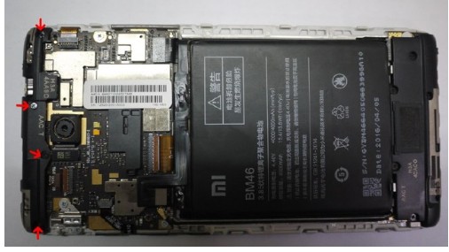
Remove the 4 screws at the arrow in the figure below.
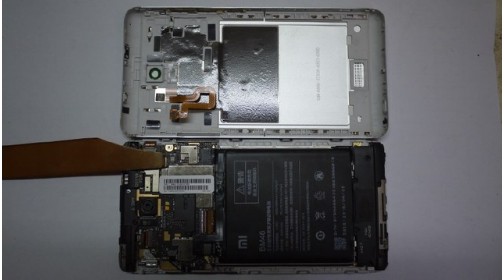
Use an opening pick to pry out the motherboard cover.
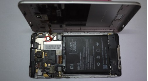
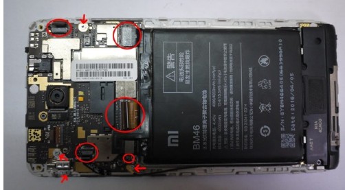
Disconnect the 4 connecting wires at the red circle and pry out one of the wires at the small red circle. Then remove the 4 screws at the arrow.
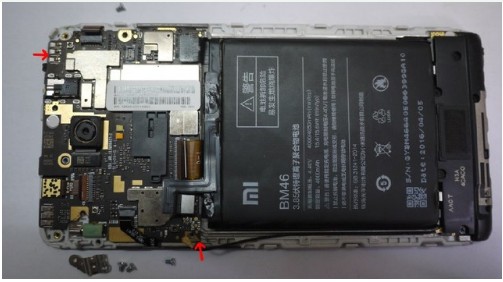
Pry the motherboard up from the arrow and pull it out slowly. Note that there is adhesive tape under the rear camera, just pull the motherboard up.
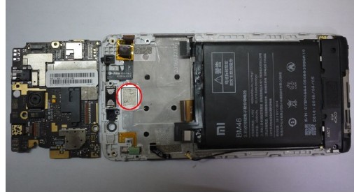
The motherboard is removed. The red circle in the picture below is glued to the heat dissipation copper of the motherboard under the rear camera. Not glued to the camera.
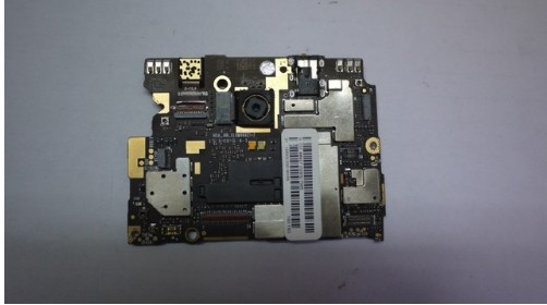
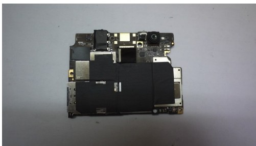
The front view of the motherboard, with the words 16G on it.
The back of the motherboard, the large black layer is the heat dissipation copper of the motherboard.
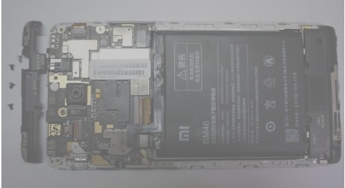
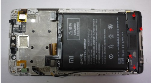
Next, remove the tail plug cover and remove the 5 screws at the arrow in the figure below.
Use an opening pick to pry out the cover.
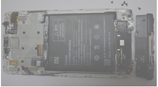
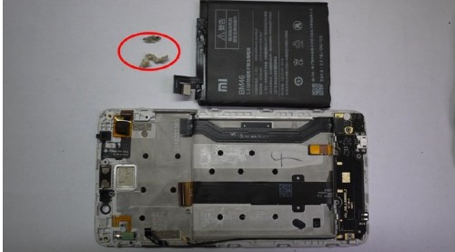
Next, disassemble the most difficult battery. The battery is glued with white glue. You need to use 2 opening picks to slowly insert the white glue into the place. Insert the white glue and the bottom plate. Pay attention to the data cables on both sides, don't disconnect them.
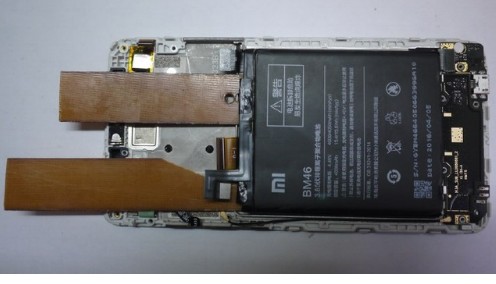
The battery is pried out. The red circle is the removed white glue. The other tail plugs, vibrators, and earpieces are all covered with double-sided tape, and can be removed by slowly prying them.
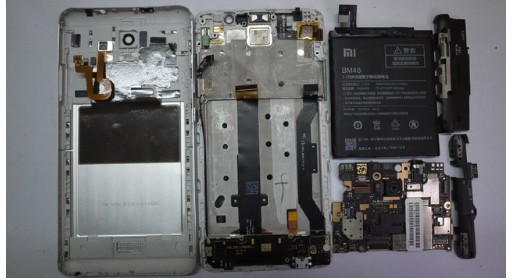
Finally, a picture of the family with the parts removed from this mobile phone.
Innosilicon is a worldwide one-stop provider of high-speed mixed signal IPs and ASIC customization with leading market shares in Asian-Pacific market for 10 consecutive years. Its IP has enabled billions of SoC's to enter mass production, covering nodes from 180nm to 5nm across the world`s foundries including: GlobalFoundries, TSMC, Samsung, SMIC, UMC and others. Backed by its 14 years of technical expertise in developing cutting-edge IPs and ASIC products, Innosilicon has assisted our valued partners including AMD, Microchip and Microsoft to name but a few, in realizing their product goals.
Innosilicon team is fully devoted to providing the world's most advanced IP and ASIC technologies, and has achieved stellar results. In 2018, Innosilicon was the first in the world to reach mass production of the performance-leading GDDR6 interface in our cryptographic GPU product. In 2019, Innosilicon announced the availability of the HDMI v2.1 IP supporting 4K/8K displays as well as our 32Gbps SerDes PHY. In 2020, we launched the INNOLINK Chiplet which allows massive amounts of low-latency data to pass seamlessly between smaller chips as if they were all on the same bus. With a wide range of performance leading IP in multiple FinFET processes and 22nm planar processes all entering mass production, Innosilicon's remarkable innovation capabilities have been proven in fields such as: high-performance computing, high-bandwidth memory, encrypted computing, AI cloud computing, and low-power IoT.
Innosilicon Miner:Innosilicon A4+ LTCMaster,Innosilicon A6+ LTCMaster,Innosilicon A6 LTCMaster
Ltcmaster,innosilicon ltcmaster,innosilicon ltc miner,Innosilicon a4,Innosilicon a6
Shenzhen YLHM Technology Co., Ltd. , https://www.asicminer-ylhm.com