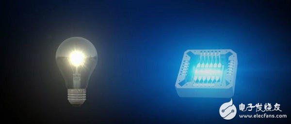
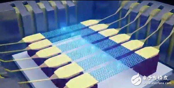
The simplest artificial light source can be integrated into the chip surface
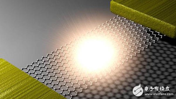
Recently, a joint team of researchers from Columbia University, Seoul National University (SNU) and the Korea Institute of Standards and Sciences (KRISS) reported that they achieved graphene luminescence for the first time (graphene has only one atomic thickness, It is the ideal crystal form of carbon) - made the world's thinnest light bulb. The team attached small pieces of graphene to the metal electrode, suspended it above the substrate material and loaded it with a certain current to heat it.
The thinnest light bulb in the world
Yun Daniel Park, a professor of the Department of Physics and Astronomy at the National University of Korea, said that the material used in this study is the same material that Edison used to invent incandescent bulbs in the same year: "Edison originally tried to use carbon materials. As the filament of the incandescent lamp in his experiment, now we are back to the same element. But the difference is that we use the pure form of carbon - graphene material, and reach its thickness limit - —An atomic thickness.†James Hone, a professor of mechanical engineering at Columbia University, one of the principals of the research group, said: “We can say that we have made the world's thinnest light bulb. The new 'broadband' source can be integrated onto silicon chips, paving the way for atomic thickness, collapsible and transparent background display technology, and graphene-based silicon-based optical communication technology."
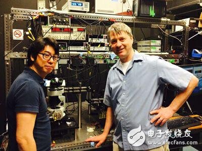
Professor Young Duck Kim and Professor James Hone
Illumination in the tiny structure of the chip surface can ultimately lead to a fully integrated "photonic circuit" that uses light to replace the current role currently used in semiconductor circuits. Previously researchers have tried many different technical solutions, but have never succeeded in integrating the oldest and simplest artificial light source, the incandescent bulb, onto the surface of the chip. By measuring the spectrum of the graphene material source, attaching the graphene microfilament to the metal electrode and then suspending it on the silicon substrate, the current is passed through the filament and heated to over 2500 ° C (4500 ° F), enough to make it bright Visible light.
The researchers used graphene to make the world's thinnest on-chip light source. The first author of the study, Young Duck Kim, a postdoctoral fellow at the University of Columbia's Professor Horn, said: "From this monoatomic thickness of graphene material. The visible light intensity is very high, even without using any amplification equipment, it can be seen directly with the naked eye."
This foldable flexible light source also meets the requirements of optical communication
Interestingly, the spectrum of the source shows that it will peak at a particular band, which the team found was because light from the graphene material and light that penetrated the graphene material and was reflected by the surface of the silicon chip appeared. Interference phenomenon. Kim pointed out: "The reason for this is because the graphene material is transparent, which is different from any material traditionally used as a filament, so that we can adjust the emission spectrum by adjusting the spacing between the graphene material and the substrate material. Types of."
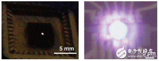
Optical (left) and microscopic (right) images of visible light emitted from suspended graphene materials
The reason why graphene can achieve such high temperatures without causing the melting of surrounding materials or metal electrodes is due to its interesting nature. As the graphene material heats up, it becomes more and more hot. conductor. This means that the high temperatures it has will be confined to a very small "hot spot" area.
Kungs senior researcher Myung-Ho Bae said: "At the highest temperatures, the electron temperature is much higher than the acoustic vibration mode of the graphene lattice, so only less energy is needed to achieve visible-light luminescence. These unique thermal properties This allows us to heat the graphene material to half the temperature of the sun's surface and achieve a luminous efficiency 1000 times higher than conventional filament materials.†At the same time, the team also demonstrated the future scalability of the technology – They implemented graphene emitters based on large scale chemical vapor deposition (CVD).
Currently, the research team is conducting further research to improve the performance of this technology. For example, how fast such a light source can be switched to meet the requirements of optical communication? There is also a need to develop techniques to enable integration into foldable substrate materials. Horn said: "We have just begun to develop the use of this material. For example, this technology can be used to develop micro-heating plates, which can be heated to thousands of degrees Celsius in an instant to help with high-temperature chemical reactions or Catalytic research."
Boiler Pressure Gauge,Inflatable Pump Pressure Gauge,Mini-Sized Theromanometer Pressure Gauge,Gauge Pressure
ZHOUSHAN JIAERLING METER CO.,LTD , https://www.zsjrlmeter.com