Analysis of 56 common technical terms for DAC and ADC
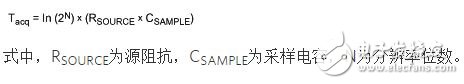
Acquisition time
The acquisition time is the time required from the release hold state (performed by the sample-and-hold input circuit) to the 1 LSB range where the sample capacitor voltage is stable to the new input value. The formula for the acquisition time (Tacq) is as follows:
Aliasing
According to the sampling theorem, the input signal frequency exceeding the Nyquist frequency is the "aliased" frequency. That is, these frequencies are "folded" or copied to other spectral locations near the Nyquist frequency. To prevent aliasing, all unwanted signals must be sufficiently attenuated so that the ADC does not digitize them. Aliasing can be an advantage when undersampling.
Aperture delay
The aperture delay (tAD) in the ADC is the time interval from the sampling edge of the clock signal (the rising edge of the clock signal in the figure below) to the time the sample is taken. Sampling is performed when the tracking-and-hold of the ADC is switched to the hold state.
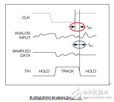
Aperture jitter
Aperture jitter (tAJ) is the change in aperture delay between sample and sample, as shown. Typical ADC aperture jitter values ​​are much smaller than the aperture delay values.
Binary coding (unipolar)
Standard binary is an encoding method commonly used for unipolar signals. The binary code (zero to full scale) ranges from all 0 (00. .000) to all 1 positive full scale values ​​(11..111). The intermediate value is represented by a 1 (MSB) followed by a full 0 (10..000). This encoding is similar to offset binary encoding, which supports both positive and negative bipolar transfer functions.
Bipolar input
The term "bipolar" means that the signal oscillates at a certain reference level. In a single-ended system, the input is usually referenced to the analog ground, so the bipolar signal is a signal that swings above and below the ground level. In a differential system, the signal is not ground referenced, but the positive input is referenced to the negative input, and the bipolar signal is the positive input signal above and below the negative input signal.
Common mode rejection (CMRR)
Common mode rejection is the ability of a device to reject a common-mode signal from two inputs. The common mode signal can be an alternating or direct current signal, or a combination of both. The common mode rejection ratio (CMRR) is the ratio of the differential signal gain to the common mode signal gain. CMRR is usually expressed in decibels (dB).
Crosstalk
Crosstalk indicates how much each analog input is isolated from other analog inputs. For ADCs with multiple input channels, crosstalk is the total amount of signal coupled from one analog input signal to the other, typically expressed in decibels (dB); for DACs with multiple output channels, crosstalk is Refers to the total amount of noise generated at the output of another DAC when one DAC output is updated.
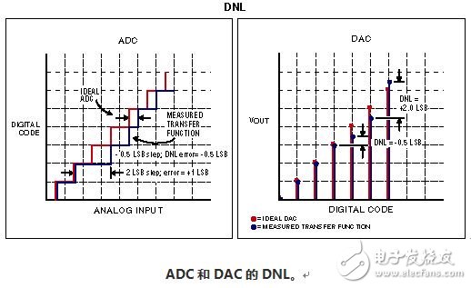
Differential nonlinearity (DNL) error
For an ADC, the difference between the analog input levels that trigger any two consecutive output codes should be 1 LSB (DNL = 0), and the deviation of the actual level difference from 1 LSB is defined as DNL. For DACs, the DNL error is the difference between the ideal and measured output response of a continuous DAC encoding. The analog output values ​​of the ideal DAC response should be strictly different by one code (LSB) (DNL = 0). (The DNL indicator is greater than or equal to 1 LSB guarantee monotonicity.) (See "Monopoly.")
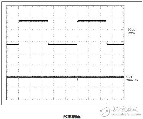
Digital feedthrough
Digital feedthrough is the noise generated at the DAC output when the DAC digital control signal changes. In the figure below, the feedthrough at the DAC output is the result of serial clock signal noise.
Dynamic Range
The dynamic range is defined as the range between the device noise floor and its specified maximum output level, usually expressed in dB. The dynamic range of the ADC is the range of signal amplitudes that the ADC can resolve; if the dynamic range of the ADC is 60dB, the resolution of the signal is from x to 1000x. For communication applications, the signal strength varies widely, and the dynamic range is very important. If the signal is too large, it will cause the ADC input to over-range; if the signal is too small, it will be submerged in the quantization noise of the converter.
Effective number of bits (ENOB)
ENOB represents the dynamic performance of an ADC at a specific input frequency and sample rate. The error of an ideal ADC contains only quantization noise. As the input frequency increases, the overall noise (especially the distortion component) also increases, thus reducing ENOB and SINAD (see "Signal to Noise + Distortion Ratio (SINAD)"). The ENOB of the full-scale, sinusoidal input waveform is calculated by:
Load-induction output
A measurement technique that applies a voltage (or current) at the far end of the circuit and then measures (detects) the resulting current (or voltage). For example, a DAC with an integrated output amplifier sometimes contains a load-sensing output. The output amplifier provides an inverting input for external connections and the feedback path must form a closed loop externally.
Full power bandwidth (FPBW)
The analog input signal applied while the ADC is operating is at or near the specified full-scale voltage of the converter. Then increase the input frequency to a certain frequency to reduce the amplitude of the digital conversion result by 3dB. The input frequency is the full power bandwidth.
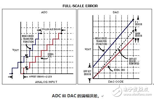
Full frame (FS) error
The full-scale error is the difference between the actual value of the trigger transition to full-scale encoding and the ideal analog full-scale transition value. The full-scale error is equal to “offset error + gain error†as shown in the figure below.
FS gain error (DAC)
The full-scale gain error of a digital-to-analog converter (DAC) is the difference between the actual and ideal output spans. The actual span is the difference between the output when the input is set to all 1s and the input is set to all 0s. The full-scale gain error of all data converters is related to the reference chosen to measure the gain error.
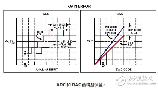
Gain error
The gain error of the ADC or DAC represents how well the slope of the actual transfer function matches the slope of the ideal transfer function. Gain error is usually expressed as a percentage of the LSB or full-scale range (%FSR) and can be eliminated by hardware or software calibration. The gain error is equal to the full-scale error minus the offset error.
Gain error drift
Gain error drift refers to the change in gain error caused by ambient temperature, usually expressed in ppm/°C.
Gain consistency
Gain consistency represents the degree of matching of all channel gains in a multi-channel ADC. To calculate the consistency of the gain, apply the same input signal to all channels and then record the maximum gain deviation, usually expressed in dB.
Spike
A spike is a voltage transient that is generated at the output of the DAC when the MSB transitions, usually expressed as nV? s, equal to the area under the voltage-time curve.
harmonic
The harmonic of the periodic signal is a sinusoidal component that is an integer multiple of the fundamental frequency of the signal.
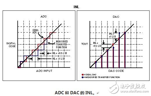
Integral nonlinearity (INL) error
For data converters, integral nonlinearity (INL) is the deviation of the actual transfer function from the line of the transfer function. After eliminating the offset error and gain error, the line is the line between the best fit line or the end of the transfer function. INL is often referred to as "relative accuracy."
Intermodulation distortion (IMD)
IMD refers to the phenomenon of new frequency components that are not present in the original signal due to nonlinearities in the circuit or device. IMD includes harmonic distortion and two-tone distortion. When measured, it is taken as the ratio of the total power of the selected intermodulation products (i.e., IM2 to IM5) to the total power of the two input signals (f1 and f2). The 2nd to 5th order intermodulation products are as follows:
· 2nd order intermodulation products (IM2): f1 + f2, f2 - f1
· 3rd order intermodulation products (IM3): 2 x f1 - f2, 2 x f2 - f1, 2 x f1 + f2, 2 x f2 + f1
· 4th order intermodulation product (IM4): 3 x f1 - f2, 3 x f2 - f1, 3 x f1 + f2, 3 x f2 + f1
· 5th order intermodulation product (IM5): 3 x f1 - 2 x f2, 3 x f2 - 2 x f1, 3 x f1 + 2 x f2, 3 x f2 + 2 x f1
Least significant bit (LSB)
In the binary number, the LSB is the lowest weighted bit. Usually, the LSB is the rightmost bit. For an ADC or DAC, the weight of the LSB is equal to the full-scale voltage range of the converter divided by 2N, where N is the resolution of the converter. For a 12-bit ADC, if the full-scale voltage is 2.5V, then 1LSB = (2.5V/212) = 610μV
MSB jump
When MSB transitions (middle scale point), MSB changes from low level to high level, all other data bits change from high level to low level; or MSB changes from high level to low level, while other The data bit changes from low to high. For example, 01111111 becomes 10000000 which is the MSB jump. MSB hopping tends to produce the most severe switching noise (see spikes).
/b"monotonous
In the sequence, if Pn + 1 is always greater than or equal to Pn for each n, then the sequence is said to increase monotonically; similarly, if for each n, Pn + 1 is always less than or equal to Pn, then say The sequence is monotonically reduced. For DACs, if the analog output always increases as the DAC code input increases, the DAC is said to be monotonic; for an ADC, if the digital output code always increases as the analog input increases, the ADC is said to be It is monotonous. If the converter's DNL error is not greater than ±1LSB, monotonicity can be guaranteed.
Most significant bit (MSB)
In the binary number, the MSB is the highest weighted bit. Typically, the MSB is the leftmost bit.
Multiplying DAC (MDAC)
The multiplying DAC allows the AC signal to be applied to the reference input. The DAC can be used as a digital attenuator by connecting the signal of interest to the reference input and using the DAC to encode the scaled signal.
No loss coding
When a ramp-up signal is applied to the analog input of the ADC, the ADC has no missing codes if the ADC generates all possible digital codes.
Nyquist frequency
The Nyquist theorem states that the sampling rate of the ADC must be at least twice the maximum bandwidth of the signal to completely recover the analog signal without distortion. This maximum bandwidth is called the Nyquist frequency.
Offset binary code
Offset binary is an encoding method commonly used for bipolar signals. In offset binary coding, the negative maximum value (negative full-scale value) is represented by all 0 (00..000), and the positive maximum value (forward full-scale value) is all 1 (11..111) ) said. The zero frame is represented by a 1 (MSB) followed by a full 0 (10..000). This method is similar to standard binary, which is commonly used for unipolar signals (see Binary Code, Unipolar).
Offset error (bipolar)
The measurement of the offset error of the bipolar converter is similar to the measurement of the offset error of the unipolar converter, but the error at the zero amplitude is measured at the midpoint of the bipolar transfer function (see offset error unipolar)
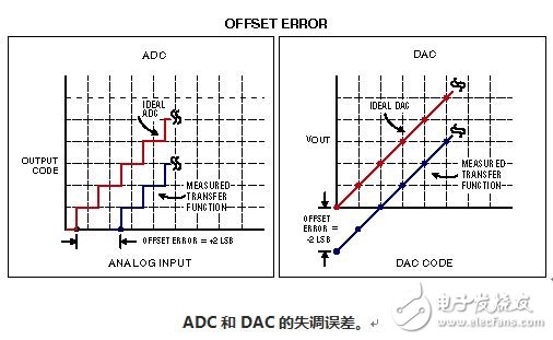
Offset error (unipolar)
The offset error is often referred to as the “zero amplitude†error, which is the difference between the actual transfer function and the ideal transfer function at a certain operating point. For an ideal data converter, the first transition occurs at 0.5 LSB above zero. For the ADC, apply a zero-voltage to the analog input and increase until the first transition occurs; for the DAC, the offset error is the analog output when the input code is all zeros.
Offset error drift
Offset error drift refers to the change in offset error caused by ambient temperature, usually expressed in ppm/°C.
Oversampling
For an ADC, if the frequency of the sampled analog input is much higher than the Nyquist frequency, it is called oversampling. Oversampling effectively reduces the noise floor, so the dynamic range of the ADC is increased. Increasing the dynamic range in turn increases the resolution. Oversampling is the basis of a sigma-delta ADC.
Phase matching
Phase matching represents the degree of phase matching of identical signals applied to all channels of a multi-channel ADC. Phase matching refers to the maximum phase offset in all channels, usually expressed in degrees.
Power supply rejection ratio (PSRR)
Power Supply Rejection Ratio (PSRR) is the ratio of the change in supply voltage to the change in full-scale error, expressed in dB.
Quantization error
For an ADC, the quantization error is defined as the difference between the actual analog input and the digital code representing the value (see "Quantization").
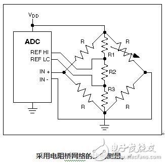
Proportional measurement
The voltage applied to the ADC voltage reference input is not a constant voltage, but is proportional to the signal applied to the transmitter (ie, the load cell or bridge). This type of measurement is called a proportional measurement, which eliminates all errors caused by changes in the reference voltage. The method of using the resistance bridge in the figure below is an example of proportional measurement.
Resolution
The ADC resolution is the number of bits used to represent the analog input signal. In order to reproduce the analog signal more accurately, it is necessary to increase the resolution. Using a higher resolution ADC also reduces quantization errors. For DACs, the resolution is similar: the higher the resolution of the DAC, the smaller the step produced at the analog output when encoding is increased.
Effective value (RMS)
The RMS value of the AC waveform is the effective DC value or the equivalent DC signal of the signal. When calculating the RMS value of the AC waveform, the AC waveform is squared and time averaged, and then the square root is taken. For a sine wave, the RMS value is 2/2 (or 0.707) times the peak value, which is 0.354 times the peak-to-peak value.
Sampling rate/frequency
The sample rate or sampling frequency is expressed in "samples per second" (sps) and refers to the rate at which the ADC acquires (samples) the analog input. For ADCs that perform a sample per conversion (such as SAR, Flash ADC, or pipelined ADC), the sample rate is also referred to as throughput. For sigma-delta ADCs, the sampling rate is generally much higher than the data output frequency.
Setup time
For DACs, the settling time is the time interval from the command to update (change) its output value to the time the output reaches its final value (within a specified percentage). The settling time is affected by the slew rate of the output amplifier and the total amount of amplifier ringing and signal overshoot. For the ADC, the time required for the sampling capacitor voltage to settle to 1 LSB is less than the capture time of the converter.
SINAD
SINAD is the ratio of the RMS value of a sine wave (the input of the ADC, or the output recovered by the DAC) to the RMS value of the converter noise plus distortion (no sine wave). RMS noise plus distortion includes all spectral components except the fundamental and dc offsets below the Nyquist frequency. SINAD is usually expressed in dB.
Signal to noise ratio (SNR)
The signal-to-noise ratio (SNR) is the ratio of the wanted signal amplitude to the noise amplitude at a given point in time. The larger the value, the better. For waveforms that are perfectly reconstructed by digital sampling, the theoretical maximum SNR is the ratio of the full-scale analog input (RMS value) to the RMS quantization error (residual error). Ideally, the theoretical minimum ADC noise contains only the quantization error and is directly determined by the resolution of the ADC (N bits):
(In addition to quantization noise, the actual ADC also generates thermal noise, reference noise, clock jitter, etc.)
Signed binary code
In the signed binary encoding method, MSB represents the sign of a binary number (positive or negative). Therefore, the 8-bit representation of -2 is 10000010, and the representation of +2 is 00000010.
Slew rate
The slew rate is the maximum rate at which the DAC output changes, or the maximum rate at which the input change to the ADC digital output is not erroneous. For DACs with an output amplifier, the specified slew rate is usually the slew rate of the amplifier.
Small signal bandwidth (SSBW)
To measure the small signal bandwidth, an analog input signal of sufficiently small amplitude is applied to the ADC whose slew rate does not limit the performance of the ADC. Then, the input frequency is scanned until the amplitude of the digital conversion result is reduced by 3 dB. Small signal bandwidth is often limited by the performance of the associated sample-and-hold amplifier.
Spurious free dynamic range (SFDR)
The spurious-free dynamic range (SFDR) is the ratio of the RMS amplitude of the fundamental (signal component maximum) to the RMS value of the second largest spurious component (excluding dc offset). SFDR is expressed in decibels (dBc) relative to the carrier.
Total harmonic distortion (THD)
The distortion component of the THD measurement signal is expressed in decibels (dB) relative to the fundamental. For ADCs, Total Harmonic Distortion (THD) is the ratio of the RMS of the harmonics of the selected input signal to the fundamental. When measuring, only harmonics within the Nyquist limit are included.
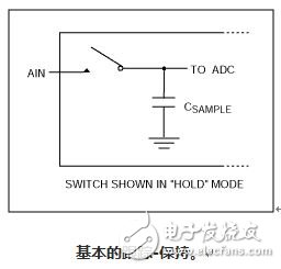
Track-and-hold
Track-and-hold is often referred to as "sampling-holding" and refers to the input sampling circuit of the ADC. The most basic representation of the trace-and-hold input is the analog switch and capacitor (see figure). When the switch is closed, the circuit is in "tracking" mode; when the switch is open, the sampling capacitor maintains the last transient value of the input and the circuit is in "hold" mode.
Conversion noise
Conversion noise refers to the range of input voltage variations that cause the ADC output to switch between adjacent output codes. When the analog input voltage is increased, the voltage that triggers the hopping (encoding edge) of each code is undefined due to the associated transient noise.
Twos complement code
The two's complement encoding method is used for positive and negative encoding, simplifying addition and subtraction calculations. In the encoding method, the 8-bit representation of -2 is 11111110, and the representation of +2 is 00000010.
Undersampling
In undersampling techniques, the ADC sampling rate is lower than the analog input frequency, which will cause aliasing. According to Nyquist's theorem, it is natural to know that undersampling will lose signal information. However, if the input signal is properly filtered and the analog input and sampling frequency are properly selected, the aliasing component containing the signal information can be moved from a higher frequency to a lower frequency and then converted. This method effectively uses the ADC as a downconverter to move higher bandwidth signals to the effective bandwidth of the ADC. For this technology to be successful, the bandwidth of the ADC track-and-hold circuit must be able to handle the expected highest frequency signal.
Unipolar
For single-ended analog input ADCs, the unipolar signal input range is zero (typically ground) to full scale (usually the reference voltage); for differential input ADCs, the signal input range is zero to full scale, with a positive input equivalent The input range is measured at the negative input.
Zero error
See offset error (unipolar).
10Kv Steel Pole,Metal Pole,Steel Pole
Jiangsu Baojuhe Science and Technology Co.,Ltd. , https://www.galvanizedsteelpole.com