KA3842 notebook power adapter switching power supply circuit
Some electronic enthusiasts who have just been involved in maintenance often find that these notebook adapters with switching power supplies are more complicated and cannot be repaired. In fact, the internal circuit design of the power adapters of different brands and different models of notebook computers and LCD monitors is basically the same. For beginners, as long as they master a typical principle of such switching power supply, it is not difficult to repair the rocker. In the following, this article uses a typical adapter that uses the KA3842 control chip in a notebook and LCD power adapter as an example to illustrate its working principle and maintenance method. Figure 1 shows the circuit schematic of the adapter switching power supply. Figure 2 shows the pin function of the Samsung power supply control chip KA3842 used in the power supply.
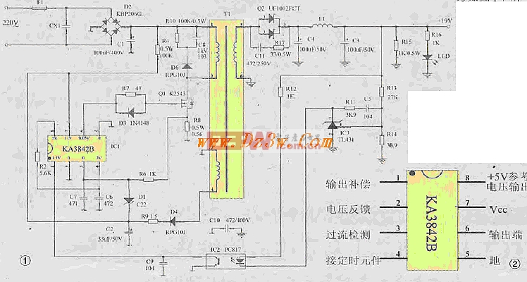
First, the basic working principle of the circuit The power adapter completes the function of converting 220V AC voltage into 19V DC voltage output, and the output current is about 3A. The basic working process of the circuit is as follows: 220v AC input voltage is rectified by bridge rectifier circuit D2 (KBP206G), and C1 is filtered to obtain DC voltage of about 300v. This voltage is added to the field effect switch tube through the 1~2 winding of switching transformer T1. Ql (K2543) D pole, the other way is stepped down by R4 to get about 17V starting voltage to power ICl (KA3842) 7 pin, and generate 5V reference voltage from ICl internal reference generator output from pin 8, at this time inside The oscillator starts to oscillate. From the 6th pin, the widening pulse (PWM) is output, and the switching transistor Q1 is driven to operate in the switching state. The D-pole output current of Q1 generates an induced voltage on the Tl primary winding, and is coupled to the magnetic core. The TI secondary, the induced voltage generated on the secondary 5 -6 winding is rectified and filtered by Schottky diode Q2 and capacitor C4 to obtain a 19v DC voltage output. In order to ensure the output voltage is stable, the output terminal is subjected to error sampling of the 19V output voltage by R13 and R14. The sampling voltage is compared and error amplified by the three-terminal adjustable shunt reference IC3 (TL431), and the photoelectric coupler IC2 (pC817) is driven. The error voltage is amplified and sent to the inside of the first pin of ICl (KA3842). The width of the output pulse of pin 6 is changed by the internal PWM circuit to change the switching time of Q1, so as to adjust the output voltage. After such a feedback control process, the output voltage is finally stabilized at 19v. There are also several overvoltage and overcurrent protections in the circuit: 1. The induced voltage of the primary 3-4 winding of the switching transformer is rectified and filtered by D4 and C2. A voltage of about 17v is sent to the 7th pin of Icl to maintain the normal operation of IC1 (the voltage of 300V is supplied to the 7 pin of R4 step-down supply because the current is small as the starting voltage). When the output voltage rises due to some reason, The voltage of the circuit will also rise. When the voltage rises above 22v, the Zener diode D1 will reverse breakdown, causing the voltage of the overcurrent protection terminal of IC1 pin 3 to rise above 1V. At this time, the IC will be turned off internally. The pulse output of the 6th abdomen stops the circuit and achieves the purpose of overvoltage protection. 2. When the current of the switch Q1 is too large for some reason, the voltage across the S1 pole of the Q1 will increase, and when the voltage rises high, the voltage of the IC1 pin 3 is high. It will also cut off the output of pin 6 of IC1 to protect against overcurrent. 3. The R10, C8, and D6 connected to the D pole of the switch Q1 form a spike absorption loop, which absorbs the spike induced pulse generated on the 1-2 winding of the T1 during the Q1 cutoff period to prevent the Q1 from being broken down.
Dance Floor Led Display,Dance Floor Led Screen,Led Screen Dance Floor,Led Dance Floor For Sale
ShenZhen Megagem Tech Co.,Ltd , https://www.megleddisplay.com