CMOS development of RF transceivers for multimode applications
Users need smaller and cheaper phones, get fast service and more features in handheld devices. This is driving the industry to accelerate innovative solutions and reduce costs to get products to market as quickly as possible. This added pressure allows manufacturers to reconsider the technology to solve these problems.
Silicon technology and integrated key component units such as RF transceivers reduce product size and cost.
The stringent performance requirements of cellular standards such as GSM have previously limited RF transceiver integration, forcing alternative technologies such as SiGe BiCMOS or bipolar. Now, the popularity of GSM/GPRS CMOS transceivers has increased, making the choice of CMOS RF technology more mature.
Despite the powerful and convincing benefits of CMOS RF transceiver design, design engineers must overcome structural and circuit design issues when developing handheld WCDMA, EDGE, GPRS/GSM standard highly integrated multimode transceivers. It is worthwhile to invest time and effort in the development of RF transceivers for multimode applications in CMOS. The market answer is also positive.
Multi-mode development trend
To enable global operators to accommodate different cellular architectures, handset manufacturers have combined multiple wireless cellular technologies (multi-mode) into one device to provide the best point of sale for a particular market. For example, the number of handsets supporting EDGE on the market has increased and is backward compatible with GSM/GPRS services. Similarly, in the future, 3G mobile phones will support WCDMA in addition to EDGE/GPRS/GSM technology. Global roaming requires five frequency bands: GSM-850MHz, E-GSM-900MHz, DCS-1800MHz, PCS-1900MHz and UMTS-2100MHz. Mobile phone designers must consider all of these requirements and meet user requirements for low cost and form factor products.
Silicon integration and module integration facilitate multi-mode functionality. Most multimode platforms combine separate wireless subsystems, for example, multimode phones supporting GSM/GPRS and WCDMA can have a WCDMA transceiver with GSM/GPRS transceivers, as well as RF front-end and passive component units to support two Modes and bands (see Figure 1). This method is most practical because the GSM/GPRS and WCDMA channel bit rates are based on different reference clock frequencies (13MHz/26MHz and 19.2MHz, respectively). A typical GSM/GPRS transmitter structure (such as OPLL) cannot be directly added to WCDMA. In this example, reducing the number and cost of multimode design components requires higher levels of integration and innovative RF technology.
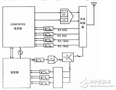
Figure 1. Typical 3G multimode/multiband RF design with separate 3G and 2G wireless technologies
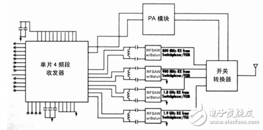
Figure 2 Block diagram of a single 4-band GSM/GPRS CMOS transceiver
Multi-RF front-end system integration solution
The RF front-end design of the 4-band GSM/GPRS system is shown in Figure 2, using a highly integrated single-chip CMOS transceiver. The antenna switch module is connected to the transmit and receive paths, and the receiver SAW filter and associated matching circuitry are used for each GSM band. The transmit path requires at least two PAs: one PA for the GSM-850MHz and E-GSM-900MHz bands and the second PA for the 1.8GHz DCS and 1.9GHz bands.
Many of the integrated RF front-end modules available reduce component count and simplify design. They include modules for power amplifiers and power control logic (PA modules) and transmitter modules with PA and switching functions. At the receiving end, it consists of a SAW filter unit and an RF front-end module with a multiplexer and a receive filter.
Compared to the GSM/GPRS system in Figure 2, the more complex front-end design of the Figure 1 3G multimode system supports 2.5G and 3G RF signal transmission. Adding a multiplexer is necessary because WCDMA is based on frequency division duplexing, and the transmitter and receiver are simultaneously switching. However, like GSM/GPRS, economic scaling will bring front-end component integration.
Today's cellular base station architectures fall into two categories: baseband functions are split into discrete analog and digital baseband chips or monolithic highly integrated CMOS SoC devices (including implementation modes and digital functions). Because each method has distinct advantages, choosing between the two methods of distribution depends on factors such as choosing a future integration route for most economic platform scenarios.
Although the monolithic approach saves the true area of ​​the PCB, the use of separate analog and digital baseband chips is the most desirable path for integration because it isolates the analog baseband functionality from the "pure" digital circuitry that implements the digital baseband. The two-chip solution also enables the digital baseband to scale smaller CMOS geometries while integrating its CMOS platform components (eg, application processor, image processor, memory)
One trend in baseband architecture is to simply remove the analog baseband chip, thereby optimizing the digital baseband functionality and simplifying the wireless to baseband chip interface design. This method uses a high speed digital interface between the wireless and digital baseband. This interface can be specified as serial or parallel. The serial interface reduces the number of device pins but increases the number of transistors on the cache chip. Parallel interfaces increase pin count and package size, but are more efficient in silicon.
The DigRF Standards Body now specifies a standard high-speed serial interface specification for 2.5G (see Figure 3). Wireless design adds complexity when supporting digital interfaces. It must not only perform analog to digital and digital to analog conversions, but must also have interface logic to handle baseband digital communications. These functions are implemented more easily and economically than other processes using CMOS process technology.
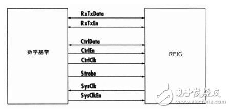
Figure 3 2G DigRF interface between wireless and digital baseband
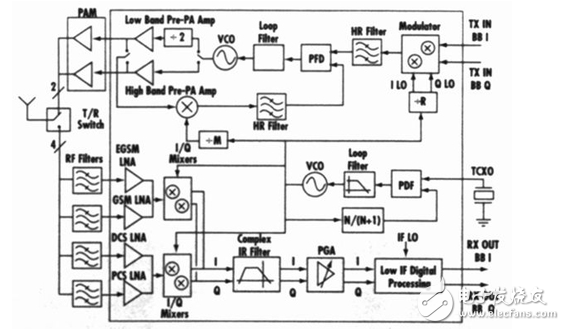
Figure 4 Single-chip 4-band CMOS transceiver block diagram
CMOS advantages
Implementing transceivers in CMOS technology has the following advantages:
CMOS has a lower wafer cost structure at equal process sizes compared to SiGe BiCMOS processes.
CMOS allows chip fabrication in multiple manufacturers using standard processes.
According to Moore's Law, CMOS designs can scale smaller process sizes.
CMOS enables RF-enabled digital circuits, resulting in a highly programmable design that enables small chips, high manufacturability, and good robustness.
CMOS transceivers can integrate other functions (such as DigRF interface or digital baseband functionality) to form a single RF and baseband component.
CMOS has proven to be a technology for implementing transceivers, and manufacturers have produced a large number of GSM/GPRS, WLAN and Bluetooth radios.
The choice of transceiver architecture for multimode GSM/GPRS/EDGE/WCDMA handsets is a key decision. Integration is now especially important in many monolithic CMOS GSM/GPRS transceivers, typically integrating VCOs, frequency synthesizers, loop filters, and DCXO. High integration helps ensure good wireless performance because critical functions are shielded from external noise sources.
BT Battery,Speaker Battery,BT Speaker Battery,Bluetooth Speaker Battery
Shenzhen Sunwind Energy Tech Co.,Ltd , https://www.sunwindbatterylm.com