How to make some trade-offs in PCB board design to make PCB's power distribution network reasonable
When designing a more complex board, you must make some design trade-offs, and these trade-offs will have some factors that affect the design of the PCB's power distribution network.
When the capacitor is installed on the PCB board, there will be an additional loop inductance, which is related to the installation of the capacitor. The size of the loop inductance depends on the design, and the size of the loop inductance depends on the line width and line length of the line from the capacitor to the via. The length of the trace is the length of the connecting capacitor and the power/ground plane, the distance between the two holes, the diameter of the hole, the pad of the capacitor, and so on. Figure 1 shows the installation graphics of various capacitors:
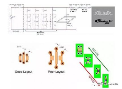
Figure 1 The best and worst capacitor layout
Design points to reduce the inductance of the capacitor loop
â– The hole should be placed as close as possible to the capacitor. Reduce the power/ground hole spacing. If possible, use multiple pairs of power/ground holes in parallel. For example, place two holes with opposite current polarity as close as possible, and place holes with the same current polarity as far as possible.
â– Use short and wide traces to connect holes and capacitor pins.
â– Place the capacitors on the surface of the PCB (top and bottom), as close as possible to their corresponding power/ground planes, so as to reduce the distance between the holes. Use a thin electrolyte between power/ground.
For the installation of the capacitor and the propagation inductance, the following is the design of three different situations. Figure 2 shows the introduction of loop inductance in various design situations:
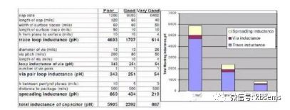
Figure 1 The best and worst capacitor layout
Situation 1-poor design
â– Designers do not pay attention to the design of power distribution network (PDN).
â– The hole spacing is not optimized.
â– The distance between the power supply and the ground plane is not optimized.
â– The wiring distance between the hole and the capacitor pin is long.
As for the size of the entire loop inductance, the loop inductance mainly comes from the wiring, because compared with the other two cases, the line length of the poor design is 5 times of them (good design and very good design). The distance from the bottom of the installed capacitor to the nearest plane is also the main factor in the size of the loop inductance, because this is not optimized (10mil), and the wiring has a great influence on the size of the entire loop inductance. Similarly, because the designer uses a 10mil dielectric material between the power supply and the ground, the secondary factor of loop inductance comes from the propagation inductance. The effect of not optimizing the distance between the vias is not so significant relative to the length of the small hole, and the influence of the hole will become greater with longer vias.
Situation 2-good design
â– Designers paid attention to the design of part of the power distribution network (PDN).
â– The spacing of the holes has been improved, and the length of the holes remains the same.
â– The distance between the power supply and the ground plane has been improved.
â– The routing distance between vias and capacitor pins has been optimized.
The loop inductance of the trace is still the main contributor to the overall loop inductance. The trace loop inductance of a good design is about 2.7 times smaller than that of a poor design, because the designer reduced the thickness of the dielectric from 10 mils to 5 mils, and the propagation inductance is reduced by half. As the distance between the vias is reduced, the influence of the vias has been slightly improved.
Situation 3-very good design
â– Designers pay great attention to the design of PDN.
â– The spacing and length of holes are improved.
â– The distance between the power supply and the ground has also been fully optimized.
â– The trace distance between vias and capacitor pins has been optimized.
The inductance of a very well-designed trace is about 7.65 times smaller than that of a poorly-designed trace. As the trace length is reduced, the thickness from the bottom surface of the capacitor installation to the nearest plane layer is reduced on the PCB board, thus achieving the goal. Since the designer has optimized the thickness of the electrolyte layer between the power supply and the ground, the propagation inductance will be greatly reduced. The hole spacing and hole length are greatly reduced, and the loop inductance of the via has also been significantly improved. Compared to a poor design, the total loop inductance of a very good design is reduced due to one of the seven main factors being reduced. .
On the PCB board, additional via loop inductance is introduced through the mounting capacitor, which reduces the capacitor's resonant frequency. When you are designing a power distribution network (PDN), you must take this factor into consideration. In high-frequency design, reducing loop inductance is the only visible way to reduce impedance.
For a given power supply, compared to a very good design and a poor design, the report generated by the PDN tool shows that the PCB cutoff frequency of a very good design will be higher. This may be the opposite of the expected result, because decoupling at a higher cut-off frequency requires more capacitance than decoupling at a lower cut-off frequency.
In the case of very good designs, a higher cutoff frequency means that higher frequencies can be decoupled. The capacitors placed on the PCB have a decoupling effect on a higher frequency of noise.
In the case of a poor design, it is not possible to decouple PCB boards that exceed the lower cutoff frequency. Any additional capacitance increase, that is, adding a decoupling capacitor that exceeds the cut-off frequency can only increase the BOM cost without any influence on the decoupling effect. Compared with a very good design, for a poor design, the design of its power distribution network is more susceptible to noise at a certain frequency.
As another example, suppose a 20-layer PCB has a total thickness of 115 mils. The power layer is on the third layer. The thickness from the first layer (the layer where the FPGA is) to the third layer is 12 mils. Then the thickness from the bottom layer to the third layer is 103 mils. The power and ground layers are separated by the 3 mil dielectric. . The inductance of the BGA hole for this track is 5nH (5 pairs of holes for this power track). In order to deal with the relatively tight layout and routing area of ​​the first layer, the associated decoupling capacitors are installed on the bottom layer. Since this installation will have a long via hole, this trade-off design results in a high capacitance installation inductance value. After full optimization, the mounting inductance of the capacitor in the 0402 package on the bottom layer is 2.3nH, while the mounting inductance of the same capacitor on the first layer is 0.57nH.
In order to improve the PDN effect for the trace, you can place some high-frequency capacitors on the first layer, and at the same time put the intermediate frequency and bulk capacitors in their original positions, that is, the bottom layer. This circuit design is a cut-off solution for PDN, because high-frequency capacitors are the first response capacitors below the cut-off frequency. The effect of the capacitor depends on the total loop inductance (installation inductance of the capacitor + propagation inductance + inductance of the BGA hole) and FPGA. You can put high-frequency capacitors on the first layer and a little farther away from the FPGA. The propagation inductance of the capacitor placed outside the FPGA breakout area is 0.2nH. Compared to the original method of placing on the bottom layer, this new placement method is still beneficial because the total loop inductance (0.57nH+0.2nH+0.05nH=0.82nH) is smaller than the total inductance when placed on the bottom layer.
The propagation inductance of the PCB board is related to the design, and it exists evenly in the medium between the power supply and the ground plane. The thickness of 3mil or thinner is the best design to reduce the plane propagation inductance. You can improve the performance of PDN according to the following design guidelines.
The following is the design guidance on the importance of sequence, from the first layer to the bottom, where the design guidance on the first layer is the most important.
â– Reduce the dielectric thickness between the power supply and the ground layer. When designing the stack of the board, determine the power supply, layers, and other layers. To give an example, such as stacking PWR1-GND1-SIG1-SIG2- GND2-PWR2 is better than PWR1-SIG1-GND1-SIG2-GND2-PWR2 stack. The result of the second case is that there is no optimal design for the distance between the power supply and the ground. Such a setting will cause the large capacitance propagation inductance between PWR1/GND1 to be larger than the inductance between PWR2/GND2. You can find a typical 3mil dielectric thickness between the power and ground planes without adding extra cost. For additional performance improvement, consider a dielectric thickness thinner than 3 mils, but this will cause the cost of the PCB to rise.
■When selecting a capacitor, choose multiple capacitor values ​​instead of choosing a large capacitor of the same value to achieve the target impedance. In PDN, the impedance peak is formed by the resonance reaction. High ESR can suppress resonance at the resonance frequency, thus reducing the height of the impedance peak. At the resonant frequency of the capacitor and the impedance peak, some capacitors with the same capacitance value can cut off to reduce the ESR.
In a wide frequency range, choosing a variety of capacitor types can maintain a relatively high ESR.
â– Choose where to place high-frequency capacitors to reduce the overall loop inductance. The entire inductor is composed of the ESL of the capacitor, the mounting inductance, the propagation inductance, and the via inductance of the BGA. When placing capacitors, place high frequency capacitors first, followed by intermediate frequency and low frequency capacitors.
â– When dividing the plane, make sure that the shape of the plane is a proper square. Avoid long and narrow plane shapes, because doing so will limit the size of the current and increase the plane's propagation inductance.
â– How to place the mid-frequency and low-frequency capacitors is not so sensitive, you can place them a little farther away from the FPGA.
Weigh the situation of multi-channel design
The power trace sharing increases the complexity of the PDN, and also adds a lot of noise on the PCB and the die position. For the multi-channel situation, there are two main steps to design the power distribution solution:
1. Low frequency solution
2. High frequency solution
At very low frequencies, the first step is to ensure that the size of the VRM is suitable for handling various current needs.
Low-frequency decoupling must consider the supply current of various combined power supplies. Bulk capacitors must be selected to cover the frequency band covered by the target impedance. It is difficult to know the frequency range accurately because there is an area that exceeds the impedance curve. This is the power supply area given on the die, based on its own maximum current consumption, rather than the current consumption of the same power supply combination associated with other currents. For the design, the frequency range of bulk capacitor decoupling is estimated to be from DC to about 5~10MHz.
When sharing multiple power supplies, use this design method in a similar way through the PDN tool, but it is recommended that you decouple at the highest cutoff frequency. For the decoupling of single and shared multi-channel power supplies, this is the process to successfully realize the design of a single PDN method. This method is suitable for power circuit design with similar current requirements between power circuits. However, there are a few exceptions to this method.
In this example, the power is shared between the core power supply (Vcc) and the PCI Express hard IP Block (VccHIP) power supply. The reasons for the exception are:
â– The current of VCC will be much larger than that of VCCHIP.
â– Comparing VCC and VCCHIP, the via inductance of VCC's BGA will be much lower than that of VCCHIP.
â– Comparing VCC and VCCHIP, the cut-off frequency of VCC will be much lower than that of VCCHIP.
Therefore, in the case of power supply design, using the highest cut-off frequency decoupling at the BGA via is not applicable. As shown in Figure 3, the combined impedance curve of the VCC and VCCHIP power circuits does not meet the target impedance, which is equivalent to not complying with the cutoff frequency decoupling of VCCHIP. This is because the decoupling capacitor effect is limited.
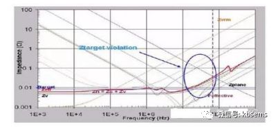
Figure 3 Cut-off frequency impedance curve of VCCHIP
According to the previous explanation, the high frequency noise in the power trace is mainly caused by its own transient current. The decoupling design guide for the highest cut-off frequency of the shared circuit is based on the impedance calculation of the entire transient current, which is a requirement of "over design".
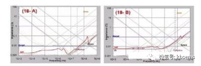
Figure 4 Changing the sharing situation of the power supply circuit
In this case, you must use the entire transient current to calculate the target impedance curve based on the PCB decoupling project, which is equivalent to the maximum current consumption at the cut-off frequency of the power circuit. In the example where the VCC and VCCHIP power circuits are shared, you must use the cutoff frequency of the VCC power circuit. Figure 3 shows the impedance curve of the combined power circuit with the cut-off frequency of the core power decoupling. For the core power supply, use the total current along the BGA ball or via (VCC+VCCHIP) to get the impedance curve. Then you can check whether the check result meets the target impedance of a single power supply design guide.
Based on the same decoupling project as Figure 4-A, Figure 4-B shows the impedance curve of the VCCHIP power supply. However, when this curve is obtained, only the current consumption and the number of BGA vias need to be considered for VCCHIP. As shown in Figure 4-B, until the cut-off frequency of the VCCHIP power supply, the impedance curve of VCCHIP has reached the target impedance.
The final decoupling project must reach the frequency of the respective target impedance. If there are some special circumstances that violate the design goals, you can adjust as little as possible to optimize the decoupling project.
In a similar situation, you can optimize any power supply combination according to the examples of VCC and VCCHIP.
On a PCB board, when there are multiple FPGAs that need to be powered from the same power supply, you can use a similar method to deal with this situation. For the design of low-frequency solutions, the total current consumption of the chip must be used, and for the design of high-frequency solutions, the current consumption of one of the chips must be used. You can use the same number of capacitors to decouple other chips at high frequencies.
When compared with the solution obtained by the field analysis tool, if the space between the two FPGA chips is relatively small, the high frequency side may lead to a slight over-design, because the field analysis tool considers the layout of the board. This may be because the chips are relatively close, and there are almost no capacitors that can cut-off to meet the location requirements of the two chips. This also depends on the cut-off loop inductance of the capacitor seen from the FPGA chip side.
A commonly used design trade-off is to establish an independent power plane, and to supply power from one power supply to different power networks, and use filters to supply clean power to the power network. In most cases, the filter is a magnetic Bead, which is connected between the two power supplies on the board. As a rule, you can provide clean power to a power network according to the following design guidelines.
â– When the magnetic beads are connected to two power supply networks, ensure that the installation inductance is the smallest.
â– Select the magnetic beads according to the characteristics listed below to ensure that the current consumption of the power supply circuit is less than the rated current of the magnetic beads.
â– Package size (0603, 0402, etc.)
â– Rated current
â– DC resistance
â– Impedance at target frequency (10 MHz, 100 MHz, 1 GHz, etc.)
â– The frequency response of the equivalent RLC model of the magnetic beads must be as consistent as possible with the given in the datasheet.
â– When doing AC analysis, in the frequency covered, the model of the magnetic bead must be included, as well as various capacitors selected to achieve the target impedance. When designing the equivalent RLC model of the capacitor, install the inductance as an integral part of the model. If the AC analysis does not have a peak in the frequency band of interest (DC to 200 MHz), you can use magnetic beads to isolate Provide clean power.
â– The PDN result obtained through the above simulation will definitely meet the target impedance requirement in the frequency band of interest.
Our company`s current transformers have high precision,wide range,small volume and good linearity that can be used to the field of electronic watt-hour meter, electric energy metering, electronic detection.
Performance
â—Power frequency insulation strength:The insulation between the primary winding and the secondary winding and the ground part of the CT can bear 4kV power frequency voltage for 1minute
â—Interturn insulation strength:The secondary open circuit, the primary winding through the rated current 1min, no inter-turn damage in the transformer
â—The deviation is better than the industry standards and national standards
High Precision Linear Ct,Useful Current Transformer,Customized Current Transformer,Durable Current Transformer
Anyang Kayo Amorphous Technology Co.,Ltd. , https://www.kayoamotech.com