Design of QPSK Modulation Circuit Based on CPLD
QPSK is a commonly used multi-ary modulation method in digital communication systems. The basic principle of its modulation: the input binary sequence is divided into groups of two symbols, and they are characterized by the four phases of the carrier. In fact, the QPSK signal is a two-way orthogonal double-sideband signal. Nowadays, people are increasingly demanding communication, high speed, large capacity, and multi-service, which pose a big challenge to limited spectrum resources. Therefore, the research on phase shift keying is of great significance. Due to the limitation of channel conditions, most digital communication systems use frequency shift keying, phase shift keying and corresponding derivative modulation methods which are insensitive to amplitude fluctuations.
Based on the above QPSK modulation, this design is based on CPLD using phase selection method to achieve modulation.
1. QPSK modulation principle
The sinusoidal carrier of the QPSK signal has four possible discrete phase states, each carrier phase carrying two binary symbols (00, 01, 10, 11), the signal representation of which is shown in Figure 1 (a) is the initial phase of the carrier is 0 ° The QPSK signal vector diagram, as shown in Figure 1(b) above, is a vector diagram of the QPSK signal with an initial phase of 45°.
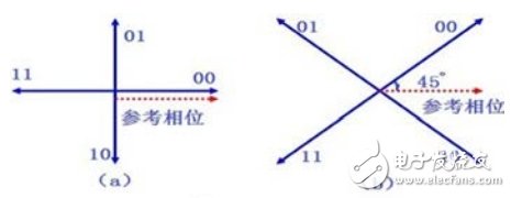
Figure 1 QPSK modulation has two production methods: multiplication circuit method and phase selection method.
Multiplication circuit modulation: The binary code is divided into two half-rate bipolar codes by the serial-to-parallel converter, and the two signals are low-pass filtered, respectively multiplied by two mutually orthogonal carrier signals, and then the two signals are added together. QPSK signal.
Phase selection method: input binary data is serial/parallel-converted to output two-bit symbols, four-phase carrier generator outputs four different phase carriers, and logic phase selection circuit converts input double-bit symbols according to serial/parallel conversion The time interval is selected as the output of one of the phases, and then the band-pass filter is used to filter out the out-of-band interference signal to obtain the QPSK modulated signal.
2. The design modulation principle
The phase selection method is used in the design. The QPSK signal has four states (00, 01, 10, 11), and the input binary sequence is divided into two groups of symbols.
In the scheme, four phases are represented by four waveforms (Fig. 2).
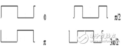
Figure 2 shows four phases in four waveforms.
3. System module design
The circuit is divided into 6 parts:
The first part: the power circuit, providing 5V voltage for the entire circuit;
The second part: the clock signal circuit, used to generate a 4MHz clock;
Part III: Baseband signal generation circuit, generating five serial codes (all 0 code, all 1 code, 0\1 code, 7-bit M sequence and 15-bit M sequence);
The fourth part: modulation circuit, the baseband signal is modulated into a sampled signal output;
The fifth part: D / A conversion circuit, the signal outputted by the modulation module is converted into an analog signal output;
The sixth part: the filter circuit, after the D/A converted analog signal is filtered to complete the analog signal reconstruction.
3.1 Power Module
There are many design solutions for providing 5V voltage to the circuit. For example, a 5V voltage can be used to provide a DC regulated power supply. The design of the DC stabilized power supply must first adopt the power transformer through the rectifier circuit and then filter the final voltage regulator. The design is relatively complicated to implement. In the design, the 9V output power supply is purchased, and the 9V power supply is converted into a 5V power supply. The circuit consists of a 7805 chip and two capacitors. The 1805 of the 7805 is connected to the power supply voltage input, the 2 pin is grounded, and the 3 pin is regulated to output 5V. C1 and C2 are used to filter out ripples.
3.2 Clock Signal Module
The clock circuit module consists of two inverters, and the crystal oscillator is oscillated with one capacitor and two resistors to generate a 4MHz clock.
3.3 baseband signal generation module
The function of this module is to generate five baseband signals (all 0 codes, all 1 codes, 0\1 codes, 7-bit M sequences, and 15-bit M sequences).
3.4 D/A module
The signal modulated by the modulation module is a digital baseband signal, which needs to be converted into an analog signal by D/A. In the design, DAC0832 is used to realize D/A conversion.
The DAC0832 outputs current, but the output is required to be voltage, so the circuit must also be converted to a voltage by an op amp.
3.5 Filter Module
The filter circuit is designed with a voltage-controlled voltage source low-pass filter. Its cut-off frequency is 50KHz, the gain is 2, K=5.
4. Modulation signal simulation
The simulation results of the modulated signal are as follows:
When 0/1 code is input, since the register y is 2, the cyclic output level is 005A7FBF.FFBF7F5A simulation waveform is shown in Fig. 3.
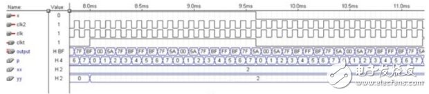
image 3
When the 15-bit M-sequence code is input, since the register y value is changed, the output level is not cyclic, and the simulated waveform is as shown in FIG.
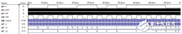
Figure 4
5. Conclusion
The main hardware modules of this design include baseband signal generation module, modulation module, D/A conversion module and filter module. Among them, the power supply module is designed to simplify the design. The power supply module is powered by 5V battery. The baseband signal generation module and modulation module are the key points in the design. Point and difficulty, based on CPLD design, CPLD is a highly integrated logic logic component. It has the characteristics of high integration, so it has the advantages of improved performance, increased reliability, reduced PCB area and low cost.
Sollid state lead battery,OPZV lead free batteries,VRLA Tubular Gel Battery,100kw off grid solar system cost,100kw hybrid solar system,hybrid solar wind system
EMoreShare International Trade (Suzhou) Co., Ltd , https://www.emoreshare.com